Chipcards Explained
by BillSF
You paid for your chipcard and it is rightfully yours!
Here are some hints to test the card and find out its secrets. The synchronous card is fully static. You can single-step the clock and record the characteristics accordingly (see schematic for special reader/writer).
The analog characteristics are extremely important. "Analog" in this context means timings, rise times, and characteristics of the I/O at different phases of the process.
While the exact timings and content of last year's cards will be explicitly detailed, you want to be able to keep up with the game and analyze cards from other countries before you get there. In other words, if your emulation does exactly what the official version does, your "card" is therefore the real thing in all respects.
Introduction
In the following pages we will explore chipcards, their types and possibilities.
All information in this piece is public, either from international documents or derived from the card itself as in the case of the analysis of the Dutch and French phonecards. No laws were broken in obtaining this information and it is expected that the reader will consider this a new area to hobby with. Criminal use of this information is on the criminal himself and in no way do we encourage fraudulent use or damage to existing systems. It will be up to the user to decide what uses of the emulator are ethical or legal. There is presently questionable software available for the smart card "inverse reader" on the Internet.
Some of you will find that spent phonecards make very secure keys for electric locks. More ambitious hobbyists will want to experiment with true processor cards. In this case the manufacturer will provide software tools to program the card. It will be up to the individual to develop their own system. In the meantime the "inverse reader" can be used to emulate existing chip masks.
Tools to do this may be available from manufacturers of chips for cards. Prices of smart cards can be as little as $2 for ones with simple processors and small memory to over $15 for chips that can handle RSA, have larger memories, and overall better security. In any case the minimum order is likely to be over 100 cards. Small quantities of conventionally packaged chips (DIL-8) can be obtained for development. All processor cards are capable of crypto. It is suggested that openly available systems like DES and IDEA be used to secure the cards. On the more expensive cards, you can implement PGP! If you try to implement your own "black box" it will surely be cracked unless you have a great deal of expertise in this rather obscure and closed field.
This article is geared towards the hardware aspect of chipcards. It will be up to the reader to obtain or write software tools. The schematics are for "professional quality" industry standard tools. You will save hundreds of dollars by building your own! The designs are strictly mine and any commercial use will be considered an infringement.
While the original scope of this article was to cover the memory cards or, simply put, "dumb cards," it is generally agreed that they are obsolete. PTT's will continue to use them for years to come, but in the more developed world, a changeover is likely to occur soon. Holland, Germany, and France are almost surely to be first. However, just about every country except the USA has a phonecard with value on it. (It should be noted here that NYNEX is experimenting with the old-fashioned diffraction grating cards once in common use in Europe. Also note that the system of billing for a call is not readily compatible yet in North America.)
We will begin with a comprehensive analysis of memory cards and their workings. From this information it will be possible to emulate them. We will discuss security tactics used to discourage this. The sharp reader will learn that it is easier to emulate a "dumb card" than to read/write one. The intelligence is in the card reader along with all the safeguards, which include things like "wire detection," "swallowing the card," and "blacklisting" abused series numbers.
Chipcards
What is a chipcard to start with?
It is generally seen as the familiar phonecard seen in an ever increasing number of countries. It was first produced in France under license from Bull S.A., a well known computer firm. The information is public and is described in ISO/IEC 7816. This multi-part document describes the physical requirements of the cards and chips in the first two parts. The third supplies the recommendations for both syncronous and asyncronous chips. Other parts have been added over the years as the technology has matured.
Most people think these telephone cards are the much touted "smart cards." In fact, all prepaid telephone chipcards are just memory cards often referred to in the industry as "dumb-cards." At present manufacturers often refer to security as using different types of memory, security fuses, and special undocumented security features.
The Siemens SLE4404 is a good example of a multipurpose memory card. This is quite possibly the German phonecard which has been said to be reloadable up to 100 times. This datasheet mentions this feature, but one must know a 16-bit code to get in, which is apparently databased by Telekom. The other option is to blow a certain security fuse and the card is irrevocably single use. Pin 4 is test and Pin 8 is that fuse pin. Both become open (not connected) when the card is secured. They are the bottom contacts on eight contact modules. Many one use cards dispense with these contacts altogether.
At present there are two major types of memory card on the market. Both types have their own unique method of marking value and methods of security. The French type is probably less expensive than the German type mentioned above, has been in use longer, and is used in most countries that use chips for phones. Modern readers could read both of these memory cards and processor cards too. Either through politics or mistrust of each other's systems, most memory cards are limited to the country issued. Other prepaid card systems include three types of magnetic card and the diffraction grating card. The chips are likely to replace all of these older types. It is suspected many nations are waiting for the more secure processor type before changing over.
First came the French card for France around 1986. It used the "French position" formally called AFNOR. The ISO position came later, in 1989. The chip module was rotated 180 degrees and placed directly below, as continuing the 2.54 mm spacing. (Looking at a standard ISO card, the French position is directly above when the card is viewed in the normal horizontal position with the module to the left.) This original version was a pathetic fuse-link ROM that was quickly cracked by students. This out-dated system can be found in India and perhaps other Third World countries. Failure of both the cards and readers was very common. "Fuse-link" ROM also implies a power hungry bipolar technology where a high current pulse is needed to burn a unit.

The new card adopted the ISO position and uses a NMOS, EPROM technology. 21V +/-2.5% is applied on the Vpp pin to alter the card. The value is stored as "units" and the largest card contains 120 and perhaps 10 bonus tics. There is room for a maximum of 152 units (see memory map). The total usable memory area, fixed and changeable, is 256 bits. Included are country codes, manufacturer codes, the initial value, and the last byte contains 0xFF if the card is new.
The "Rest Of the World" version has a slightly different format in the first twelve bytes. While the old versions burned the card in a linear fashion which was provided with the number of units needed, newer versions place more tics than needed in a particular order determined by the info in the first part of the card.
A crypto algorithm determines where the places will be from the series code and possibly other areas of the first 96 bits. This algorithm is not known to the author, but is apparently a proprietary one. Its purpose is to prevent mass emulation of the cards. It can be assumed that copying one card would allow many "re-uses" until it was "blacklisted" by the system. One would of course have to change to another phone to use a copy! It is not determined how the cells are updated in France and countries that use the similar system. (Any takers? French police tactics are downright scary!) When a card is used up, there will be remaining "units."
This is like a LOTTO at its best. Which 16, or 24, or more bits are not set out of a field of 152? The apparent key length is 56-bits and the "LOTTO field" has an astronomically larger range and could act as an extension in a double crypt system. It would appear to be something like DES and perhaps as secure or more so.
The NMOS output has levels much like TTL and is compatible to it without any pull-up resistor. The French cards use an active low RST on Pin 4. The Vpp is on Pin 6 and is +5V while reading and upped to +21V to modify. Pin 2 is R/W and is low (0) unless a modification is to be made. When 1, the Vpp is expected. The CLK is Pin 3 and the "I/O" is Pin 7.
The system used in Holland is based on the German system that appeared in 1989. While the card uses a large number of possible security measures, only a few are actually checked in either country. The card operation and method of storing value are completely different than the French type (see memory map). There are 512 possible memory locations. The card itself contains much of the security. A full rundown of all security measures will be presented (see timing diagrams).
Power-On Reset: If the CLK is 0 and RST is 1, the I/O sources current. A proper reset is RST to 1, a single CLK pulse to 1 and back to 0, and then RST to 0. It has been found the card will reset when the RST falls before the CLK. This may be one of the "undocumented" security features. The I/O is the clock inverted with the addition of current sourced when the RST is 1. Rise and fall times are very fast and well under 20 ns! The sink current is twice the source current as would be expected using equally sized N and P channel fits in a CMOS arrangement.
Here is the performance of a typical card. With the RST 1 and the CLK 0, the output will source 4 mA at 4V or put another way there will be a one volt drop if 1.0 kΩ is placed from the output to ground. This is the only occurrence of this chip sourcing current. This chip (like all known CMOS chipcards) normally relies on an "open drain" output. It will pull a 1.0 kΩ resistor tied to Vcc to 0.5V. (At this point it should be noted that 6.8 kΩ is the standard value used to pull-up the output.)
On testing about 100 cards, the propagation delay between the CLK to output into +/-30 pF ranged between 18 and 20 ns for the output falling and 33 to 37 ns for the output rising with no resistive load. This is most certainly a security feature.
CLK to DATA Out: For a read, the CLK must be 1 for at least 450 ns. However, this value is transferred to a flip-flop so when CLK falls, the data is ready in about 42 ns, going from 1 to 0. The data is read through an open drain output (the I/O) and is pulled up by a 6.8 kΩ resistor in the phone. Going from 0 to 1 under ideal conditions, the propagation delay is 55 ns.
Additional rise-time formed between the 6.8 kΩ resistor and the capacitances of the card and reader are likely to add over 150 ns. The capacitance of the standard Landis+Gyr reader is about 30 pF. If this value is tightly controlled, the rise-times can reveal additional capacitance and possibly reject a defective card. A good card would be expected to have less than 10 pF at its output.
Modifying Data: A "write" is defined as changing a 1 to a 0. An "erase" is defined as putting all zeros in a lower value field to all 1's. To perform a write, an RST pulse is generated while the CLK is 0. (This pulse can be as little as 1 µS.) The clock is then specified to remain high (1) for 10 ms to allow time to zap the bit. On the actual card, this CLK pulse can also be about 1 µS, which allows the measurement of the time actually required to change the bit.
It has been found to be about 2 ms which is far shorter than the worst case specified. There is probably nothing to do with security here, except the CLK is masked out during the write period on the newer cards. A read can be performed only if the last operation was a successful write (bit changed from 1 to 0). When the CLK is once again 0, another RST pulse is applied and the CLK is specified to remain 1 for 10 ms while all eight bits of the next lower value field are changed to 1. (In other words, you cannot add more value than you removed. As each bit in a lower value field is 1/8 that of a higher value field, zapping a higher value field bit when all the lower value field bits are 0 will restore those bits.)


Series Number: Chips are made in lots of 100. Each lot has its own number. Through central administration it is possible to monitor fraud and cancel cards that appear to have been used for more than 100 times its value. In general, the machine will not care if the number is in range and not in its memory of cards to reject. While not as clever as the French method, it will serve to keep criminal and lamer abuse down!
Much of the card, like the series number, cannot be altered. There are only 36 "value bits" on most cards. (The older cards had a 1/8 cent subfield that could be written.) There are however a total of 80-bits that can be set to 0 and stay that way. Trying to write in most "forbidden" areas will do nothing, but in certain areas the card is frozen (program counter doesn't increment anymore) if a write is attempted. These all appear to be security measures that could be taken to verify a card but it is apparently never done.
Future Imperfect
The PTT will not always use dumb cards.
In fact the present system can read some basic "challenge response" cards now available. The DES-like key is stored on each card and getting the key from one card opens the whole system to the cracker. The 64-bit challenge is issued from another smart card inside the phone. Their card contains the same key as the one you own. Therefore a "randomly" generated challenge is crypted and sent to your card. Your card uses the key to decrypt this and sends the initial "random" 64-bits back to the reader on the phone. If a match has occurred, the phone will deduct the cost of a tic. This is fast enough to make each and every tic a separate transaction.
Almost every smart card system uses this method and it is only a matter of time until the keys get out. Other key distribution methods could be used to prevent the problem of keeping all one's secrets on each card. In general, the PTT will go no further than what hackers show is insecure.
Determining Card Type
The synchronous card is clocked at 50 kHz to read and has an "active high" reset.
The async card is usually clocked at 3.58 MHz and has an active low reset.
The processor card will probably not function much below 1 MHz anyway, so on this alone the machine can check for card type. There is no specified way to determine card type as the three types are greatly different. The French cards also have an active-low reset and so do some special purpose cards that are generally used as keys. In any case the differences between types is great enough that there needs to be no standard to tell them apart.
Processor Card Emulation
All the emulation must do is see the reset rise and then answer with the standard "I'm here" response. This response is expected within 11 ms, but may come as early as 112 µs. (In emulation, the RST asserts the CTS of the RS-232 port.) At this point the "card" I/O is an input (default) and waits for further instructions. In computer terms, the format is 9600 bps, start plus eight data bits, a parity bit, and two stop bits minimum.
In many systems, the "inverse reader" is used to program the card device. To do this one must know how to answer-back with a message saying; "I have more for you." At this point a whole new identity can be loaded or audits conducted. It is likely the speed will be increased to 19.2 or 38.4 kbs for "security" or time savings. Every "facility card" is different and either development of your own or leaked knowledge of present types is needed to gain entry to the card itself.
You can however reset the card and get an answer, then issue it a challenge and get a response. Improper challenges often result in getting an ASCII 'n' (for no?) back. Certain control characters will give predetermined test responses, but only properly framed (and typically 64-bit) challenges will produce a normal response. Only by knowing the system of crypto in the card and its keys can you issue a challenge and get the expected response. Of course you must then give the card an answer to its response and then you may modify its contents!
It should be noted at this time that not all cards use crypto. In the industry this is called "mag stripe emulation." The German medical card is a fine example of a non-secure system. Since the card is readable and writable in the clear, junks, for instance, can get all the dope they need with the help of a hacker.
To hack such a system all one must do is monitor the protocol between the reader and card. Inverting the I/O and connecting to the RxD pin of a ter-minal at 9600 and proper settings will expose the "conversation." To do this you need a "card" and socket to form a sort of breakout box. More sophisticated systems could segregate out what the card says and what the reader says.
RSA: End of the Road?
Each public-key card contains its own secret keys.
This is an obvious advantage to the above systems. If you probe one card, all you have done is crack that one card! (To probe a card you must have access to a clean room with tools to take apart the module, remove any protective coating, determine the type of chip, and probe it under a microscope. This is a lot of work in a non-smoking environment!)
In a realistic system, public keys would be exchanged and then a switch to "conventional crypt" would be used as RSA is vet), computational intensive. If you look at it as PGP on a chip, you got the idea!
The cost of this type of card puts this system, for most uses, in the future. On all processor cards, it is the job of the processor to keep secret information on the card. There have been many reports of being able to "glitch" a card and read out its ROM with keys! Exact details are sketchy and beyond the scope of this article.
Besides, you are likely to waste quite a few cards before you get results even if using a proven technique.
Metal Detectors, Wire Detection and Security at the Terminal
There are several possibilities to detect irregularities on cards.
Obvious are size, thickness, and surface smoothness.
Two tactics are used on the common Landis+Gyr machines to detect wires. Neither is effective if one knows what they are doing. As mentioned in the security area, there is a simple check for rise-time on an open drain output. The time to cross the CMOS threshold is approximately: 0.7 * R * C
R is 6.8 kΩ in just about any reader and C is typically 5 pF for a CMOS input and maximum of 10 pF.
A simple grid plate can check for the clock appearing where it should not. A small coil is supplied to check for the presence of wires attached, printed circuit traces, and induced signals.
In other countries, the whole card may be "swallowed" and held. This will eliminate the need to use sophisticated wire detection methods. The card is entered in the long direction and a trap door closes that is supposed to cut off or short out any attached wires. The designers of these systems didn't consider that a type of cable commonly used in consumer products and the like will slip by. It is a tough polyester ribbon with printed conductors.
Companies such as AMP will supply them in standard lengths with standard numbers of conductors. A chipcard may need a minimum of five and a maximum of eight conductors. Another approach has been to use microelectronics and build a self-contained emulator. While it may work fine in Germany or Greece it will be rejected by the metal detector in Holland.
Processor Cards
While the scope of this article was to be on synchronous cards, the ability to "talk to" (read and write) asynchronous processor cards should be considered important.
The circuitry is very simple and works with the serial port at 9600 bps. A very cheap 3.58 MHz quartz crystal supplies the clock.
Per standard, all "smart cards" answer-back at 9600 when the clock speed is 3.58 MHz. When used with the right software, one can do many things with the card, depending on how it is programmed. An inverse reader that also runs on the serial port will be described. The clock is ignored as your computer has one and simply talks to the card politely, one way at a time.
To avoid any conflict of interest, all designs are my own and may be used for any non-commercial and non-criminal purpose.
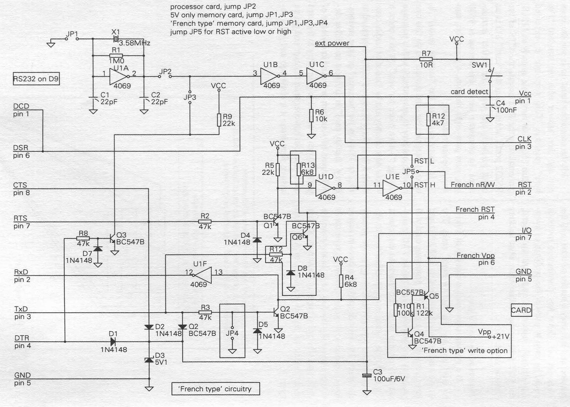
Dumbmouse Universal Reader/Writer
(Notes on Schematic)
When configured for a processor card, the 3.58 MHz crystal oscillator is allowed to run, supplying the required rate for the card to typically produce 9600 bps serial data.
While extremely simple, it is expected anyone using such a circuit will have proper prior knowledge of electronics and possibly software. The jumper options allow for variations on software and also provide the possibility of the CTS, DTR, and in some cases the TxD pins to provide the circuit power.
External power (either a hard +5V or small current applied to the Zener diode at the "ext power" input) will allow for cards that draw extreme amounts of current or added convenience in programming and/or reduction of jumper pins.
To be able to read out and write to memory cards, the 3.58 MHz will not be used and shut off (jump JP1), disconnected (open JP2), and DTR will provide for CLK pulses (jump JP3). RTS will be used to reset the card. If it is in the interest to power from the serial port, the position of JP5 should be that RST is inactive when RTS is providing power. During this reset time, the clever programmer will set TxD to provide continued power.
In the French type phonecards, TxD will provide the actual reset and JP4 will be jumped as TxD will be providing power and preventing an RxD signal otherwise. (A quick note to someone programming: a "0" sent to the serial port produces a positive voltage or "mark" condition. So when a line is said to be "providing power," a "0" is being put to that line. Conversely, what comes from the card I/O is inverted before going to the serial port. To power a card at least one and preferably two lines should be "providing power." If this is not possible for a certain card, or if the card draws heavy current, additional power must be supplied.)
JP5 is to be set so RTS is active for "most of the time." This will be fully dependent on the type of card used. For "active low" resets, as in most processor cards, RST (Pin 2) will be connected to U1 Pin 8, allowing RTS to be active while the card is active.
For active high resets, a further inversion available at U1 Pin 10 will provide a "0" when RTS is active.
To be able to write software, the programmer should have some knowledge of electronics or be within reach of someone who does. Except for writing French cards, simple code has been written to prove the concept. For French cards making RTS inactive will place +21V on Vpp (Pin 6) and +5V on the nR/W pin (Pin 2), burning the tic and making the I/O go to a "0". In no case is the I/O port used to input data on a French card.
Areas in the dashed lines apply only to French type memory cards and may be omitted if these are not of interest.
This circuit is but one example that will cover all aspects of ISO/IEC 7816. Emphasis was given to a solution requiring no special components or programming fixtures. Low-cost was also a major consideration. The card socket may be regarded by some as a "special component." They are made by ITT Cannon, Omron, and Alcatel among others. This is a new area of hobby so therefore your favorite over-the-counter parts house will almost certainly not carry them. The better distributors like Rodelco carry a full range of them. Cheaper ones (from consumer products) will ruin cards in no time and the features of the expensive types are probably not warranted for this application.
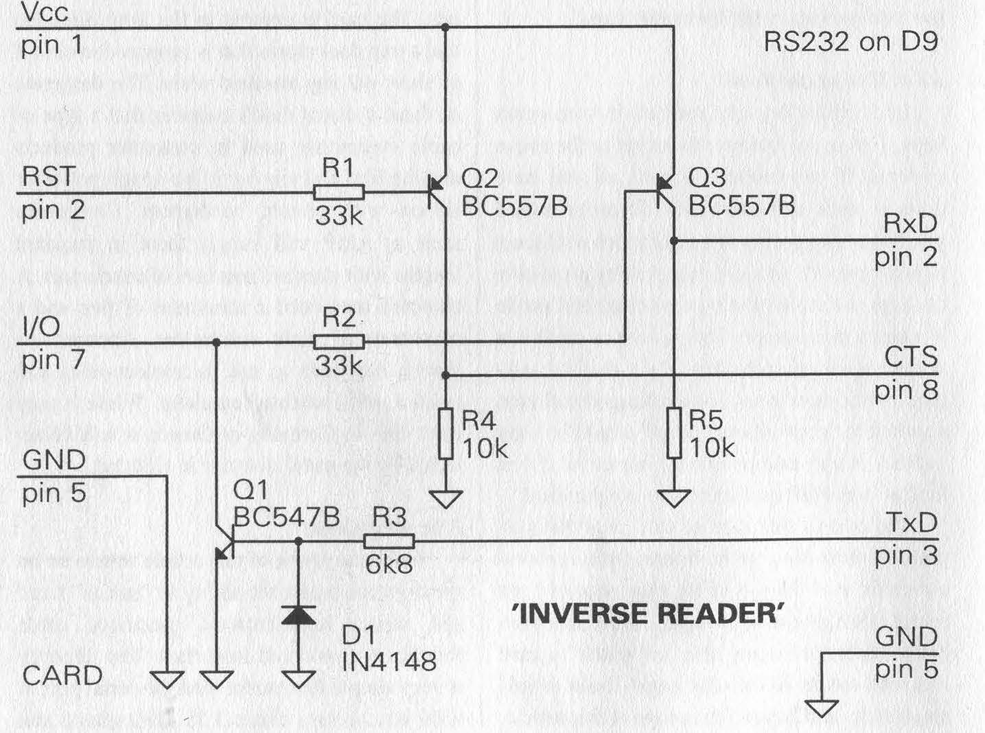
Inverse Reader Notes
The supplied schematic is for the emulation of processor type cards or to program devices that take processor cards. A special PCB could be made to bring out the four needed lines. Note the CLK is ignored and it is assumed the bit rate of the system is known. Use of a spent phonecard is a quick and cheap alternative to using a print. If using a print (PCB), it is well advised that the contacts are gold plated. In "consumer" cases, such as satellite decoders, it will be 9600 bps. The circuitry is capable of operating at any speed provided by a PC.
No schematic will be provided for synchronous card inverse readers. The clock must be brought out and all other details are supplied in the text. It is not the intent of this article to be about "free" calls.
How to Use a Spent Phonecard
The chip is a very small, approximately 1 mm square piece of silicon located directly in the center of the module.
To remove this, turn the card over and locate this point. Usually there will be an indication visible as an 8 mm circle on the back. The chip is in the exact center of this epoxy which is below the plastic. Carefully cut the bottom plastic of the card to reveal the black epoxy. The epoxy is rather soft so it can be cut down to the chip which is very hard.
Break out the chip in pieces until you reach the metal of the ground contact. At this point you could carefully solder to the top of the card and place the wires in cut grooves so they are flush to the surface.
Using low heat of about 175 degrees Celsius, you can fix the wires in the grooves or simply glue them down with epoxy. The card must maintain its constant thickness of about 0.85 mm.
If you are more ambitious, continue to carefully remove the epoxy to reveal eight contact points where the chip's bonding wires went and carefully solder from the bottom. As before, run the wires in grooves cut to the middle, bottom, or the far end of the card depending on the application. You may waste a card or two while you develop the technique, so have a few extra!

Notes on Chart
The chart (shown below) applies only to Holland, but is also related to Germany, Greece, and England, among other places.
Order of serial output reads left to right. Only the VALUE and WORM bits can be set to zero.
If a value bit of 8 units or more is written, the erase function will set all eight bits of the next lower value to 1's.
PC turns over after 512 CLK pulses and sequence repeats.
Chip powers up at bit 0 which is always 1.
Only the first 104 bits appear to be used. (0x00-0x0C)
Different types of chips may have different memory structures. All types can be identified by the first 64-bits of unalterable memory.
Byte Use Example Means 0x00 ISSUER CODE 1101 1000 PTT 0x01 LAND CODE 0011 0111 NL 0x02 SPECIFIC CODE 1111 1111 ? 0x03 MFG CODE 0010 1010 SOLAIC 0x04 INITIAL CODE 0100 1010 ü5,- 0x05 LOT CODE 1010 0001 Code assigned to 100 chips 0x06 0100 0110 0x07 (24 bits) 0001 0000 0x08 VALUE 0000 0000 4096 units per bit (last 4 only) 0x09 VALUE 0000 0000 512 units per bit 0x0A VALUE 0111 1111 64 units per bit 0x0B VALUE 0011 1111 8 units per bit 0x0C VALUE 0000 1111 1 unit per bit 0x0D VALUE 1111 1111 Non-writable 0x0E WORM 1111 1111 Any of these 16-bits can be written to 0 0x0F WORM 1111 1111 Other use? 0x10-0x17 SECURITY 1111 1111 Write attempt freezes PC until reset 0x18-0x1F SECURITY/SPARE 1111 1111 Not writable, does not freeze PC 0x20-0x27 SECURITY 1111 1111 Same as 0x10-0x17 0x28-0x2F WORM BITS 1111 1111 64 write-once bits! 0x30-0x37 SECURITY 1111 1111 Same as 0x10-0x17 0x38-0x3F SECURITY/SPARE 1111 1111 Same as 0x18-0x1F 0x00 means bits 0-7. 0x01 are bits 8-15, etc. |
Chipcard Socket Review
I have looked at several different chipcard sockets. Some are really good and inexpensive and some are unmentionably bad! ITT Cannon, Amphenol, and Alcatel all make very inexpensive "consumer" grade card sockets. All these makes come in both the "scratch the card" ($5 or less) variety and the more expensive (around $15) less scratching types. All supply both ISO position or ISO and AFNOR 16-pin sockets at slightly higher cost of course.
The above manufacturers also make consumer grade "less scratching" types where the contacts lower onto the card and only make slight scratches. A further improvement gets devices that lower the contacts directly on the module after insertion and take it up at the least tug of removing the card.
In addition to the above makers, these midrange "commercial grade" sockets are made by Omron, ddm hopt+schuler, Connectral. The "ddm" device is the superior choice with the Omron SCROJ-002 coming in second place with the others about the same. All are less than $60 list price.
If you must hold the card, try an Omron 3S4YR-SFROJ. It contains a microswitch that detects card entry, a card holding device (stronger than the card!) and a microswitch to indicate a locked down card. Red and green LEDs are provided for the user's comfort and convenience and are obviously useful! List price is about $150.
The "scratching" type is out of the question for any use that involves inserting and removing a card repeatedly (estimated module life: from 10-100 times for the cheap (phone) cards and perhaps 10 times that for the smartcards with thicker gold plating). Their intended use is similar to an IC socket (they all are IC sockets) where a card would be left in place for some time, say in a GSM or pay TV decoded. If you want to hobby with these, you'll waste a lot of cards!
That is basically what is out there for the hobbyist. I didn't go into the hyper-expensive units that "swallow" the card as they are probably not interesting to the hobbyist. There are many manufacturers of these specialized units.