| Device Description | |
| HDMI Specification | 2.0 |
| HDMI Test Type | TMDS Physical Layer Tests |
| Test Mode | Compliance Mode |
| Test Session Details | |
| Infiniium SW Version | 04.50.0008 |
| Infiniium Model Number | DSOX93204A |
| Infiniium Serial Number | MY53180105 |
| Application SW Version | 1.99.9027 |
| Debug Mode Used | No |
| Probe (Channel 1) | Model: 1169A Serial: US44000259 Head: N5380A/B Atten: Not Calibrated, Using Default Atten (2.2029E+000) Skew: Not Calibrated, Using Default Skew |
| Probe (Channel 2) | Model: 1169A Serial: US49413460 Head: N5380A/B Atten: Not Calibrated, Using Default Atten (2.0148E+000) Skew: Not Calibrated, Using Default Skew |
| Probe (Channel 3) | Model: 1169A Serial: US49412951 Head: N5380A/B Atten: Not Calibrated, Using Default Atten (2.2029E+000) Skew: Not Calibrated, Using Default Skew |
| Probe (Channel 4) | Model: 1169A Serial: US49412941 Head: N5380A/B Atten: Not Calibrated, Using Default Atten (2.1765E+000) Skew: Not Calibrated, Using Default Skew |
| Last Test Date | 2013-09-12 14:39:02 UTC -07:00 |
| Margin Thresholds | |
| Warning | < 2 % |
| Critical | < 0 % |
| Pass | # Failed | # Trials | Test Name | Worst Actual | Worst Margin | Spec Range |
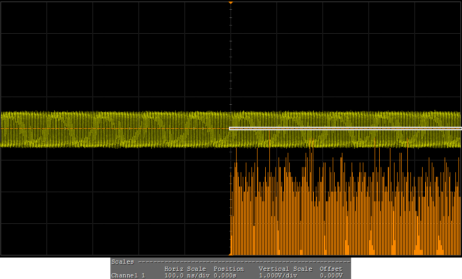
 | 0 | 1 | 7-9: Clock Jitter | 180 mTbit | 28.0 % | VALUE <= 250 mTbit |
| 0 | 1 | 7-4: Clock Rise Time | 236.575 ps | 215.4 % | VALUE >= 75.000 ps |
| 0 | 1 | 7-4: Clock Fall Time | 239.451 ps | 219.3 % | VALUE >= 75.000 ps |
| 0 | 1 | 7-8: Clock Duty Cycle(Minimum) | 49.480 | 23.7 % | >=40% |
| 0 | 1 | 7-8: Clock Duty Cycle(Maximum) | 50.100 | 16.5 % | <=60% |
| 0 | 1 | 7-10: D0 Mask Test | 0.000 | 50.0 % | No Mask Failures |
| 0 | 1 | 7-10: D0 Data Jitter | 172 m | 42.7 % | <=0.3Tbit |
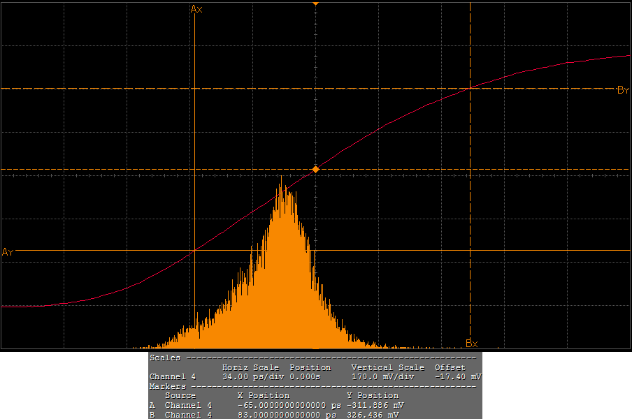
| 0 | 1 | 7-4: D0 Rise Time | 144.511 ps | 92.7 % | VALUE >= 75.000 ps |
| 0 | 1 | 7-4: D0 Fall Time | 150.023 ps | 100.0 % | VALUE >= 75.000 ps |
| 0 | 1 | 7-10: D1 Mask Test | 0.000 | 50.0 % | No Mask Failures |
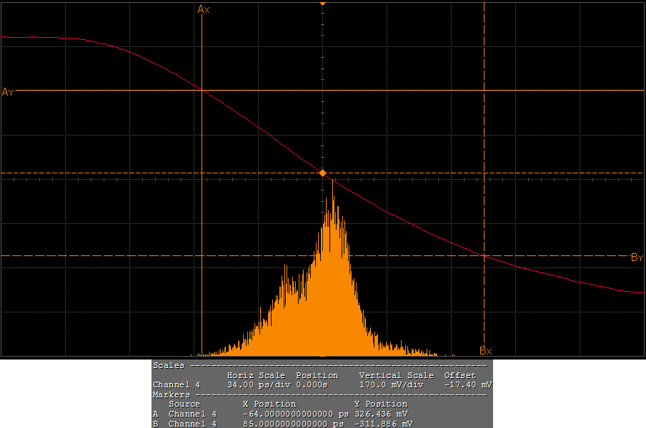
| 0 | 3 | 7-10: D1 Data Jitter | 172 m | 42.7 % | <=0.3Tbit |
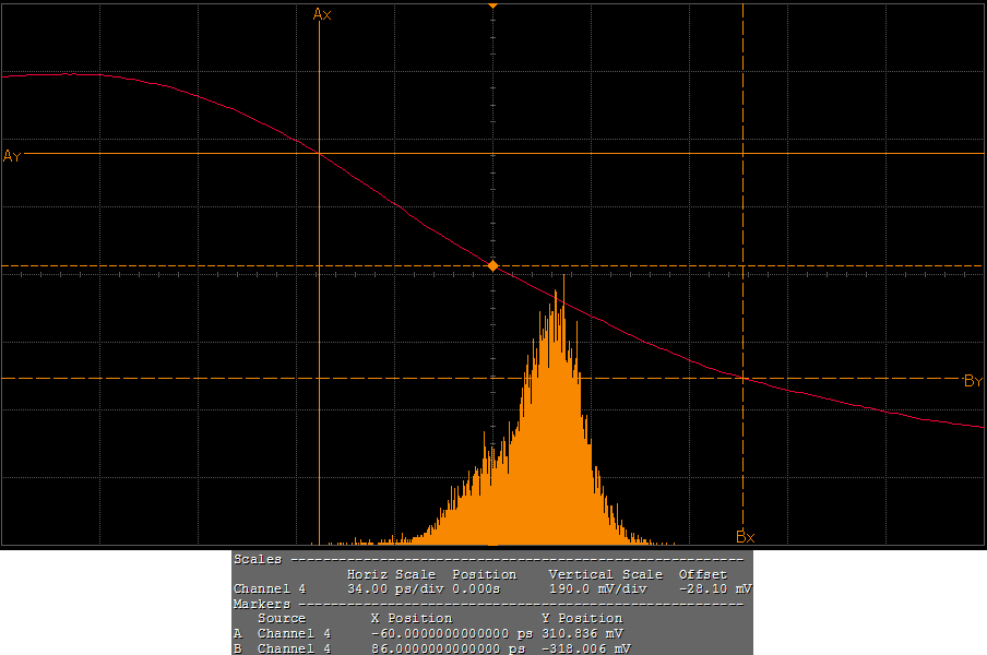
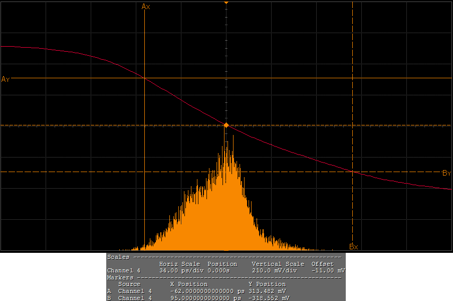
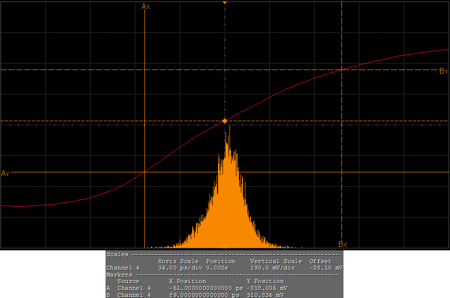
| 0 | 3 | 7-4: D1 Rise Time | 146.070 ps | 94.8 % | VALUE >= 75.000 ps |
| 0 | 3 | 7-4: D1 Fall Time | 147.491 ps | 96.7 % | VALUE >= 75.000 ps |
| 0 | 2 | 7-10: D2 Mask Test | 0.000 | 50.0 % | No Mask Failures |
| 0 | 3 | 7-10: D2 Data Jitter | 179 m | 40.3 % | <=0.3Tbit |
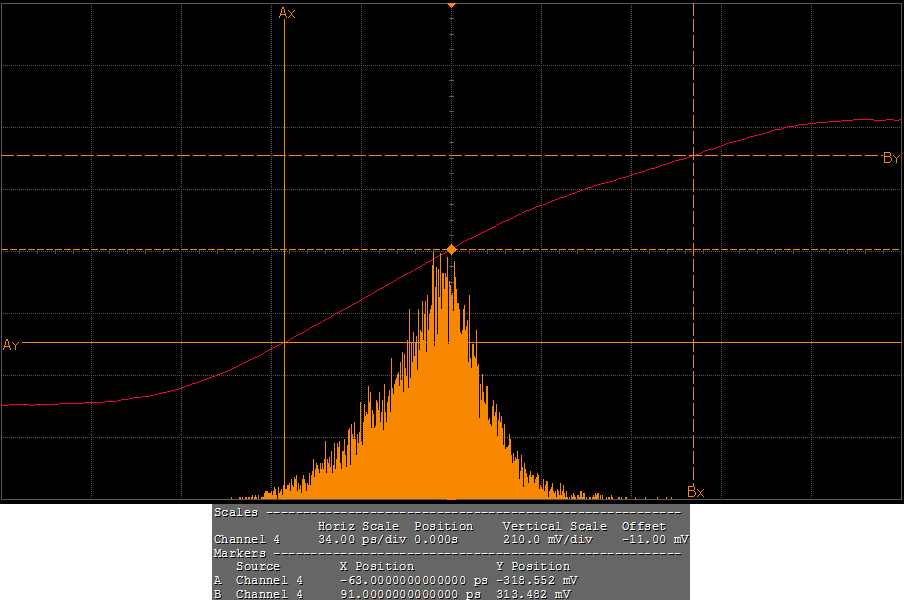
| 0 | 3 | 7-4: D2 Rise Time | 146.844 ps | 95.8 % | VALUE >= 75.000 ps |
| 0 | 3 | 7-4: D2 Fall Time | 147.883 ps | 97.2 % | VALUE >= 75.000 ps |
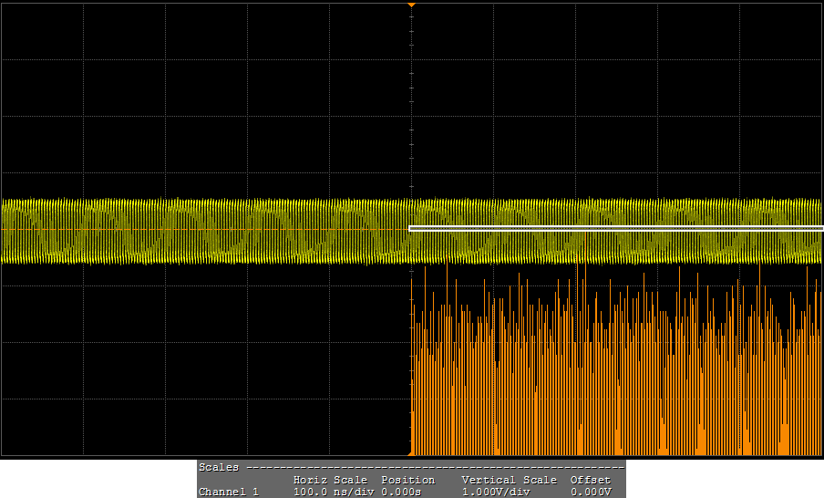
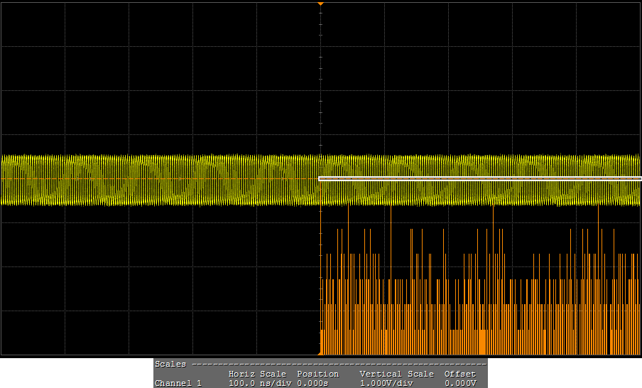
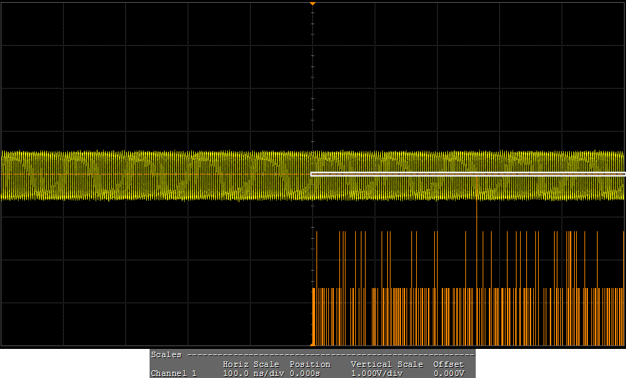
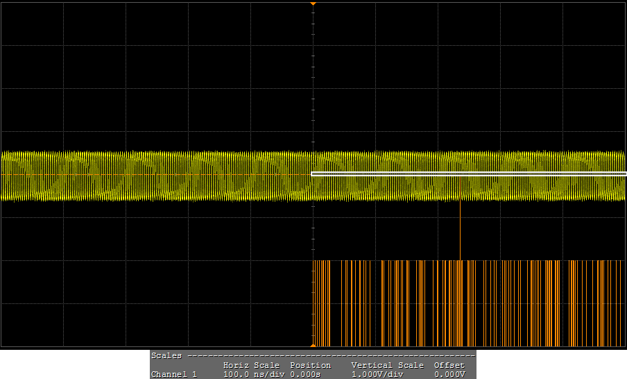
 7-9: Clock Jitter
Reference:
Test ID 7-9
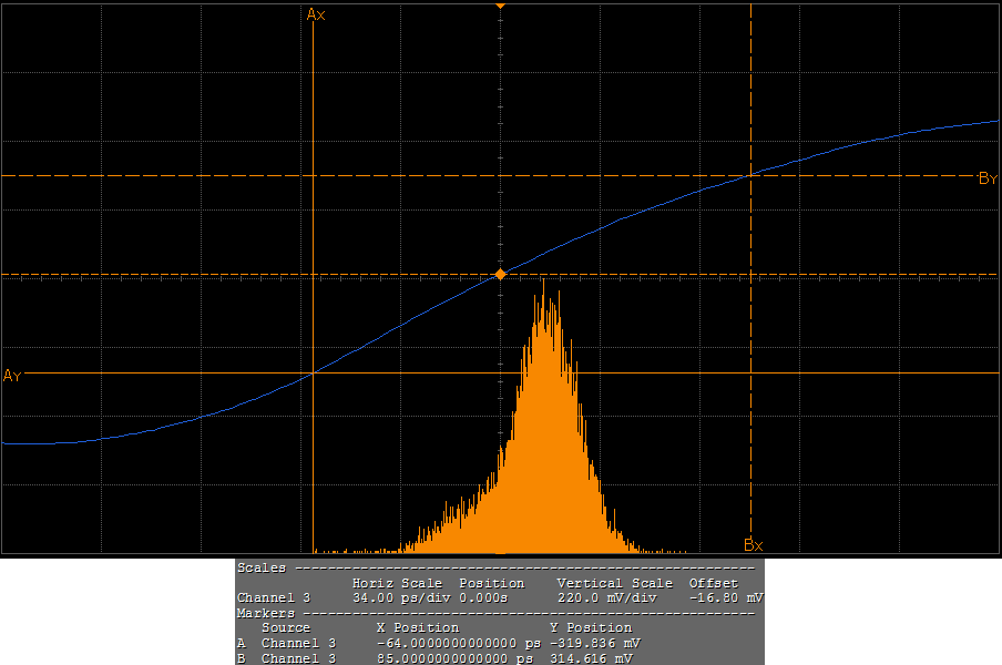
7-9: Clock Jitter
Reference:
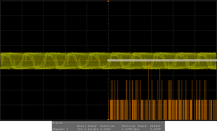
Test ID 7-9 7-4: Clock Rise Time
Reference:
Test ID 7-4
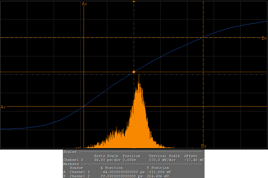
7-4: Clock Rise Time
Reference:
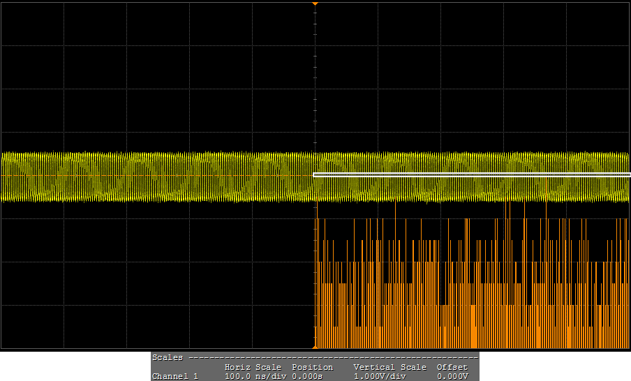
Test ID 7-4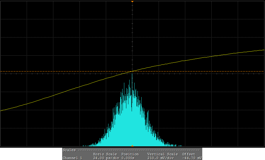 7-4: Clock Fall Time
Reference:
Test ID 7-4
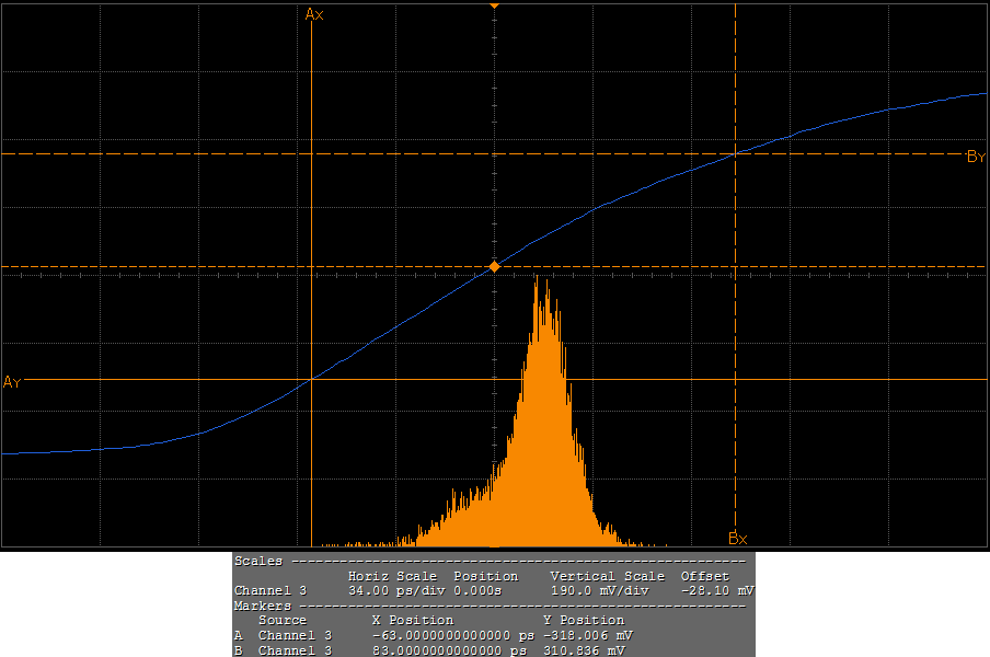
7-4: Clock Fall Time
Reference:
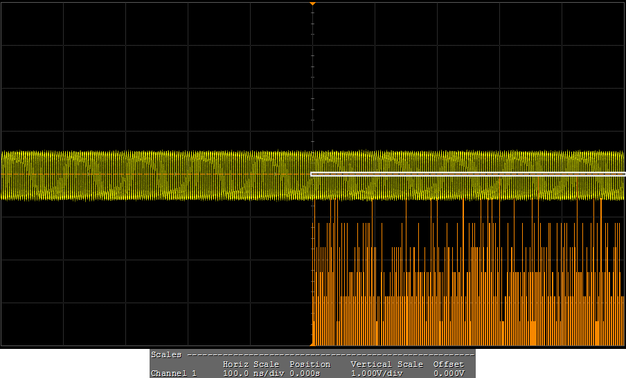
Test ID 7-4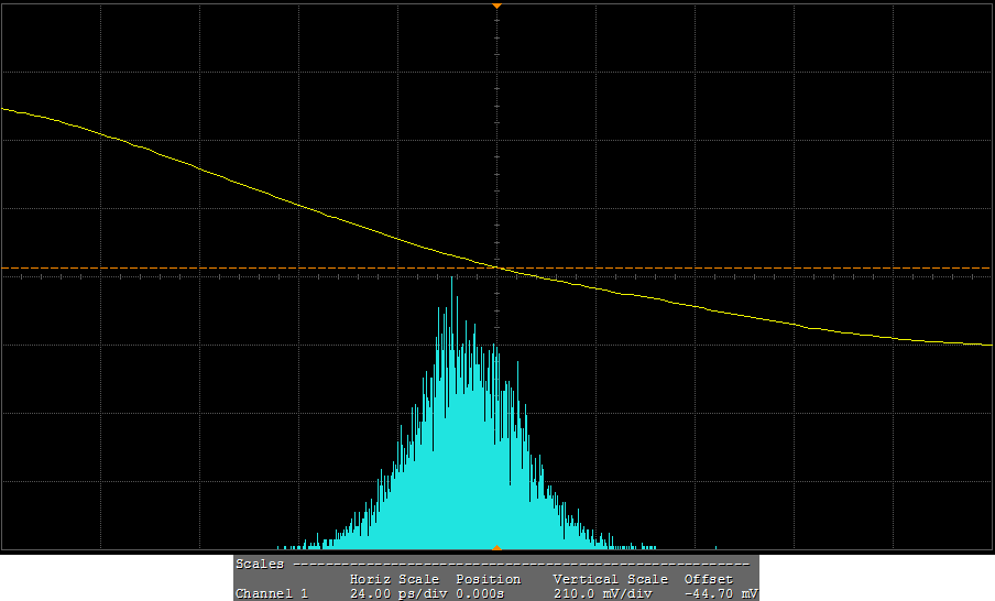 7-8: Clock Duty Cycle(Minimum)
Reference:
Test ID 7-8
7-8: Clock Duty Cycle(Minimum)
Reference:
Test ID 7-8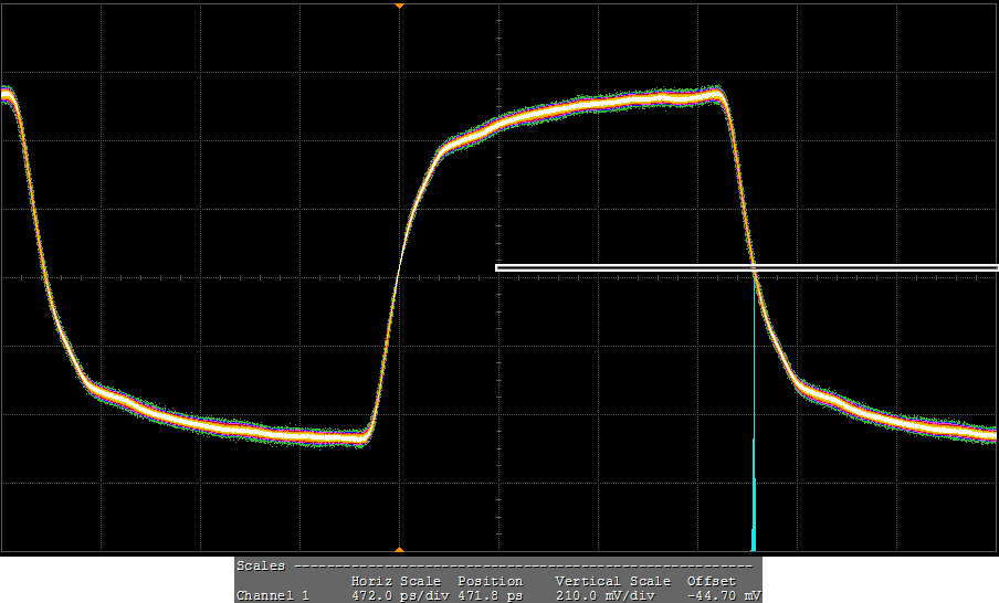 7-8: Clock Duty Cycle(Maximum)
Reference:
Test ID 7-8
7-8: Clock Duty Cycle(Maximum)
Reference:
Test ID 7-8 7-10: D0 Mask Test
Reference:
Test ID 7-10
7-10: D0 Mask Test
Reference:
Test ID 7-10 7-10: D0 Data Jitter
Reference:
Test ID 7-10
7-10: D0 Data Jitter
Reference:
Test ID 7-10 7-4: D0 Rise Time
Reference:
Test ID 7-4
7-4: D0 Rise Time
Reference:
Test ID 7-4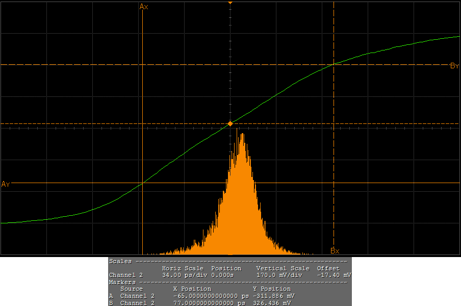 7-4: D0 Fall Time
Reference:
Test ID 7-4
7-4: D0 Fall Time
Reference:
Test ID 7-4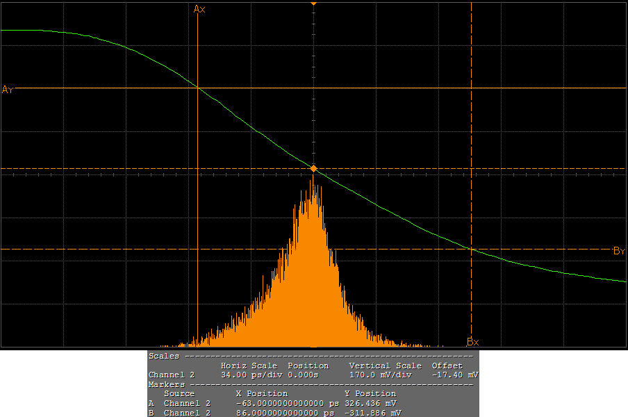 7-10: D1 Mask Test
Reference:
Test ID 7-10
7-10: D1 Mask Test
Reference:
Test ID 7-10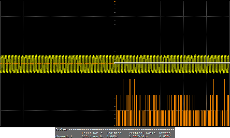 7-10: D1 Data Jitter
Reference:
Test ID 7-10
7-10: D1 Data Jitter
Reference:
Test ID 7-10| . | Trial | Actual Value | Margin | HDMIAutomationConfig | Data Lane A | Test Frequency(MHz) | Mask Moved(ps) | # Acquisitions Point | Tbit(ps) | RightJitterData(Tbit) | LeftJitterData(Tbit) | RightJitterData(ps) | LeftJitterData(ps) | Differential Swing Voltage(V) |
| Avg | 170.1 m | 43.33 % | ||||||||||||
| StdDev | 3.839 m | 1.155 % | ||||||||||||
| Range | 6.650 m | 2.000 % | ||||||||||||
| Min | 165.7 m | 42.67 % | ||||||||||||
| Max | 172.3 m | 44.67 % | ||||||||||||
| Sum | 510.2 m | 130.0 % | ||||||||||||
| Trial 1 (Worst) | 172 m | 42.7% | Timing C 2 | D1 | 296.726 | 0.000 | 16.000000000 M | 337.031 | 172 m | 172 m | 58.070 | 58.070 | 1.064 |
| Trial 2 | 172 m | 42.7% | Timing C 2 | D1 | 296.724 | 0.000 | 16.000000000 M | 337.028 | 172 m | 172 m | 58.070 | 58.070 | 1.048 |
| Trial 3 | 166 m | 44.7% | Timing C 2 | D1 | 296.664 | 0.000 | 16.000000000 M | 337.035 | 166 m | 166 m | 55.830 | 55.830 | 1.057 |
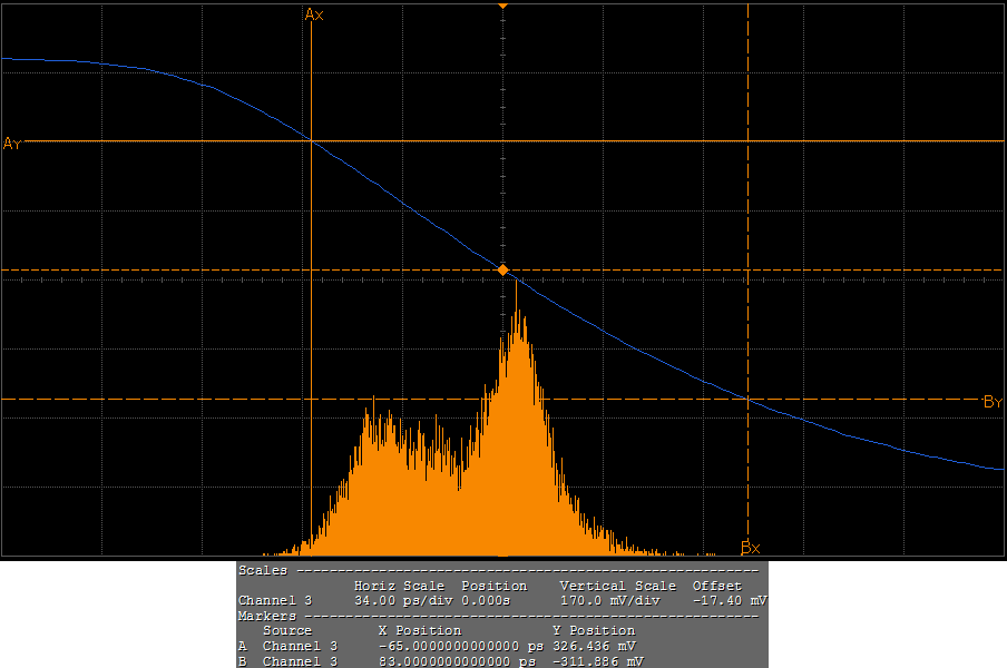
 7-4: D1 Rise Time
Reference:
Test ID 7-4
7-4: D1 Rise Time
Reference:
Test ID 7-4| . | Trial | Actual Value | Margin | HDMIAutomationConfig | Test Frequency(MHz) | Data Lane A | Upper Threshold(%) | Lower Threshold(%) | #Edge |
| Avg | 148.1 ps | 97.53 % | |||||||
| StdDev | 2.570 ps | 3.427 % | |||||||
| Range | 4.951 ps | 6.601 % | |||||||
| Min | 146.1 ps | 94.76 % | |||||||
| Max | 151.0 ps | 101.4 % | |||||||
| Sum | 444.4 ps | 292.6 % | |||||||
| Trial 1 | 151.021 ps | 101.4% | Timing C 2 | 296.726 | D1 | 80.000 | 20.000 | 15.895000 k |
| Trial 2 (Worst) | 146.070 ps | 94.8% | Timing C 2 | 296.724 | D1 | 80.000 | 20.000 | 14.189000 k |
| Trial 3 | 147.349 ps | 96.5% | Timing C 2 | 296.664 | D1 | 80.000 | 20.000 | 14.700000 k |
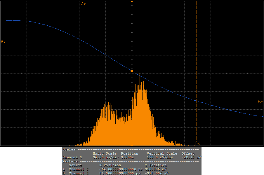
 7-4: D1 Fall Time
Reference:
Test ID 7-4
7-4: D1 Fall Time
Reference:
Test ID 7-4| . | Trial | Actual Value | Margin | HDMIAutomationConfig | Test Frequency(MHz) | Data Lane A | Upper Threshold(%) | Lower Threshold(%) | #Edge |
| Avg | 148.3 ps | 97.77 % | |||||||
| StdDev | 731.9 mps | 975.8 m% | |||||||
| Range | 1.364 ps | 1.819 % | |||||||
| Min | 147.5 ps | 96.65 % | |||||||
| Max | 148.9 ps | 98.47 % | |||||||
| Sum | 445.0 ps | 293.3 % | |||||||
| Trial 1 | 148.855 ps | 98.5% | Timing C 2 | 296.726 | D1 | 80.000 | 20.000 | 19.025000 k |
| Trial 2 (Worst) | 147.491 ps | 96.7% | Timing C 2 | 296.724 | D1 | 80.000 | 20.000 | 18.706000 k |
| Trial 3 | 148.633 ps | 98.2% | Timing C 2 | 296.664 | D1 | 80.000 | 20.000 | 19.704000 k |
 7-10: D2 Mask Test
Reference:
Test ID 7-10
7-10: D2 Mask Test
Reference:
Test ID 7-10| . | Trial | Actual Value | Margin | HDMIAutomationConfig | Data Lane A | Test Frequency(MHz) | Mask Moved(ps) | # Acquisitions Point | Tbit(ps) | RightJitterData(Tbit) | LeftJitterData(Tbit) | RightJitterData(ps) | LeftJitterData(ps) | Differential Swing Voltage(V) |
| Avg | 0.000 | 50.00 % | ||||||||||||
| StdDev | 0.000 | 0.000 % | ||||||||||||
| Range | 0.000 | 0.000 % | ||||||||||||
| Min | 0.000 | 50.00 % | ||||||||||||
| Max | 0.000 | 50.00 % | ||||||||||||
| Sum | 0.000 | 100.0 % | ||||||||||||
| Trial 1 (Worst) | 0.000 | 50.0% | Timing C 2 | D2 | 296.726 | 0.000 | 16.000000000 M | 337.031 | 172 m | 172 m | 58.070 | 58.070 | 1.064 |
| Trial 2 | 0.000 | 50.0% | Timing C 2 | D2 | 296.724 | 0.000 | 16.000000000 M | 337.028 | 172 m | 172 m | 58.070 | 58.070 | 1.048 |
 7-10: D2 Data Jitter
Reference:
Test ID 7-10
7-10: D2 Data Jitter
Reference:
Test ID 7-10| . | Trial | Actual Value | Margin | HDMIAutomationConfig | Data Lane A | Test Frequency(MHz) | Mask Moved(ps) | # Acquisitions Point | Tbit(ps) | RightJitterData(Tbit) | LeftJitterData(Tbit) | RightJitterData(ps) | LeftJitterData(ps) | Differential Swing Voltage(V) |
| Avg | 174.5 m | 41.89 % | ||||||||||||
| StdDev | 3.819 m | 1.347 % | ||||||||||||
| Range | 6.616 m | 2.333 % | ||||||||||||
| Min | 172.3 m | 40.33 % | ||||||||||||
| Max | 178.9 m | 42.67 % | ||||||||||||
| Sum | 523.5 m | 125.7 % | ||||||||||||
| Trial 1 | 172 m | 42.7% | Timing C 2 | D2 | 296.726 | 0.000 | 16.000000000 M | 337.031 | 172 m | 172 m | 58.070 | 58.070 | 1.064 |
| Trial 2 | 172 m | 42.7% | Timing C 2 | D2 | 296.724 | 0.000 | 16.000000000 M | 337.028 | 172 m | 172 m | 58.070 | 58.070 | 1.048 |
| Trial 3 (Worst) | 179 m | 40.3% | Timing C 2 | D2 | 296.663 | 0.000 | 16.000000000 M | 337.032 | 179 m | 179 m | 60.300 | 60.300 | 1.053 |
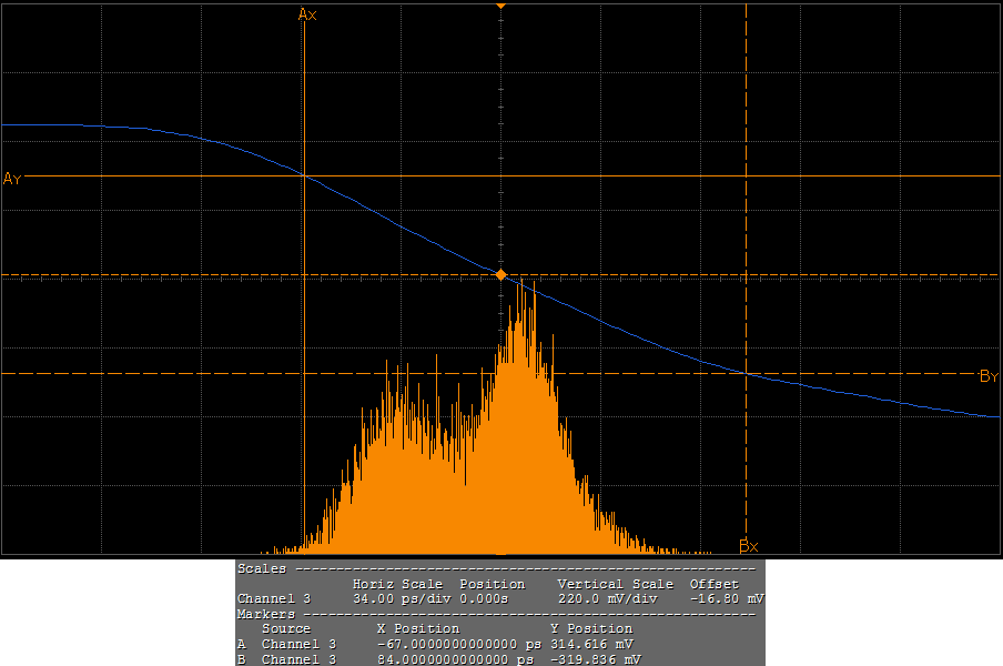
 7-4: D2 Rise Time
Reference:
Test ID 7-4
7-4: D2 Rise Time
Reference:
Test ID 7-4| . | Trial | Actual Value | Margin | HDMIAutomationConfig | Test Frequency(MHz) | Data Lane A | Upper Threshold(%) | Lower Threshold(%) | #Edge |
| Avg | 148.4 ps | 97.86 % | |||||||
| StdDev | 2.005 ps | 2.674 % | |||||||
| Range | 3.818 ps | 5.091 % | |||||||
| Min | 146.8 ps | 95.79 % | |||||||
| Max | 150.7 ps | 100.9 % | |||||||
| Sum | 445.2 ps | 293.6 % | |||||||
| Trial 1 | 150.662 ps | 100.9% | Timing C 2 | 296.726 | D2 | 80.000 | 20.000 | 18.253000 k |
| Trial 2 | 147.690 ps | 96.9% | Timing C 2 | 296.724 | D2 | 80.000 | 20.000 | 14.273000 k |
| Trial 3 (Worst) | 146.844 ps | 95.8% | Timing C 2 | 296.663 | D2 | 80.000 | 20.000 | 18.099000 k |
 7-4: D2 Fall Time
Reference:
Test ID 7-4
7-4: D2 Fall Time
Reference:
Test ID 7-4| . | Trial | Actual Value | Margin | HDMIAutomationConfig | Test Frequency(MHz) | Data Lane A | Upper Threshold(%) | Lower Threshold(%) | #Edge |
| Avg | 148.5 ps | 98.03 % | |||||||
| StdDev | 664.0 mps | 885.4 m% | |||||||
| Range | 1.325 ps | 1.767 % | |||||||
| Min | 147.9 ps | 97.18 % | |||||||
| Max | 149.2 ps | 98.94 % | |||||||
| Sum | 445.6 ps | 294.1 % | |||||||
| Trial 1 | 148.467 ps | 98.0% | Timing C 2 | 296.726 | D2 | 80.000 | 20.000 | 16.792000 k |
| Trial 2 | 149.208 ps | 98.9% | Timing C 2 | 296.724 | D2 | 80.000 | 20.000 | 14.622000 k |
| Trial 3 (Worst) | 147.883 ps | 97.2% | Timing C 2 | 296.663 | D2 | 80.000 | 20.000 | 18.031000 k |