| Device Description | |
| HDMI Test Type | TMDS Physical Layer Tests |
| HDMI Specification | 2.0 |
| Test Session Details | |
| Infiniium SW Version | 04.50.0008 |
| Infiniium Model Number | DSOX93204A |
| Infiniium Serial Number | MY53180105 |
| Application SW Version | 1.99.9025 |
| Debug Mode Used | No |
| Probe (Channel 1) | Model: 1169A Serial: US44000259 Head: N5380A/B Atten: Not Calibrated, Using Default Atten (2.2029E+000) Skew: Not Calibrated, Using Default Skew |
| Probe (Channel 2) | Model: 1169A Serial: US49412951 Head: N5380A/B Atten: Not Calibrated, Using Default Atten (2.2029E+000) Skew: Not Calibrated, Using Default Skew |
| Probe (Channel 3) | Model: 1169A Serial: US44000715 Head: N5380A/B Atten: Not Calibrated, Using Default Atten (2.2949E+000) Skew: Not Calibrated, Using Default Skew |
| Probe (Channel 4) | Model: 1169A Serial: US48470614 Head: N5380A/B Atten: Not Calibrated, Using Default Atten (2.0989E+000) Skew: Not Calibrated, Using Default Skew |
| Last Test Date | 2013-09-10 14:31:58 UTC -07:00 |
| Margin Thresholds | |
| Warning | < 5 % |
| Critical | < 2 % |
| Pass | # Failed | # Trials | Test Name | Worst Actual | Worst Margin | Spec Range |
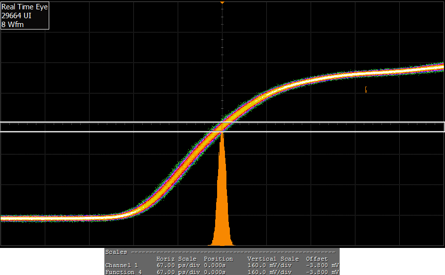
 | 0 | 3 | 7-10: D0 Mask Test | 0.000 | 50.0 % | No Mask Failures |
| 0 | 3 | 7-10: D0 Data Jitter | 47 m | 84.3 % | <=0.3Tbit |
| 0 | 2 | 7-9: Clock Jitter | 31 mTbit | 87.6 % | VALUE <= 250 mTbit |
| 0 | 1 | 7-4: Clock Rise Time | 371.934 ps | 395.9 % | VALUE >= 75.000 ps |
| 0 | 1 | 7-4: Clock Fall Time | 313.966 ps | 318.6 % | VALUE >= 75.000 ps |
| 0 | 1 | 7-8: Clock Duty Cycle(Minimum) | 49.830 | 24.6 % | >=40% |
| 0 | 1 | 7-8: Clock Duty Cycle(Maximum) | 50.140 | 16.4 % | <=60% |
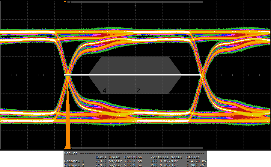
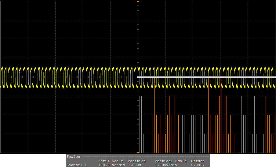
 7-10: D0 Mask Test
Reference:
Test ID 7-10
7-10: D0 Mask Test
Reference:
Test ID 7-10| . | Trial | Actual Value | Margin | Maximum Margin (s) | Maximum Margin (Vertical) (V) | HDMIAutomationConfig | Eye Width(ps) | Eye Height(mV) | Data Lane A | Test Frequency(MHz) | Mask Moved(ps) | # Acquisitions Point | Tbit(ps) | RightJitterData(Tbit) | LeftJitterData(Tbit) | RightJitterData(ps) | LeftJitterData(ps) | Differential Swing Voltage(V) |
| Avg | 0.000 | 50.00 % | 0.000 s | 0.000 V | ||||||||||||||
| StdDev | 0.000 | 0.000 % | 0.000 s | 0.000 V | ||||||||||||||
| Range | 0.000 | 0.000 % | 0.000 s | 0.000 V | ||||||||||||||
| Min | 0.000 | 50.00 % | 0.000 s | 0.000 V | ||||||||||||||
| Max | 0.000 | 50.00 % | 0.000 s | 0.000 V | ||||||||||||||
| Sum | 0.000 | 150.0 % | 0.000 s | 0.000 V | ||||||||||||||
| Trial 1 (Worst) | 0.000 | 50.0% | 0.000000000000 s | 0.000000000000 V | Not defined | 1.287000 k | 512.910 | D0 | 74.176 | 0.000 | 16.000000000 M | 1.348138 k | 47 m | 45 m | 63.000 | 60.000 | 964 m |
| Trial 2 | 0.000 | 50.0% | 0.000000000000 s | 0.000000000000 V | Not defined | 1.287000 k | 522.580 | D0 | 74.175 | 0.000 | 16.000000000 M | 1.348140 k | 47 m | 45 m | 63.000 | 60.000 | 955 m |
| Trial 3 | 0.000 | 50.0% | 0.000000000000 s | 0.000000000000 V | Not defined | 1.290000 k | 516.130 | D0 | 74.175 | 0.000 | 16.000000000 M | 1.348099 k | 42 m | 45 m | 57.000 | 60.000 | 952 m |
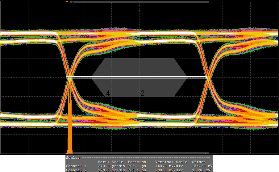
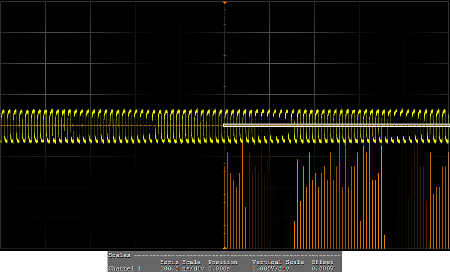
 7-10: D0 Data Jitter
Reference:
Test ID 7-10
7-10: D0 Data Jitter
Reference:
Test ID 7-10| . | Trial | Actual Value | Margin | HDMIAutomationConfig | Data Lane A | Test Frequency(MHz) | Mask Moved(ps) | # Acquisitions Point | Tbit(ps) | RightJitterData(Tbit) | LeftJitterData(Tbit) | RightJitterData(ps) | LeftJitterData(ps) | Differential Swing Voltage(V) |
| Avg | 45.99 m | 84.56 % | ||||||||||||
| StdDev | 1.284 m | 384.9 m% | ||||||||||||
| Range | 2.224 m | 666.7 m% | ||||||||||||
| Min | 44.51 m | 84.33 % | ||||||||||||
| Max | 46.73 m | 85.00 % | ||||||||||||
| Sum | 138.0 m | 253.7 % | ||||||||||||
| Trial 1 (Worst) | 47 m | 84.3% | Not defined | D0 | 74.176 | 0.000 | 16.000000000 M | 1.348138 k | 47 m | 45 m | 63.000 | 60.000 | 964 m |
| Trial 2 | 47 m | 84.3% | Not defined | D0 | 74.175 | 0.000 | 16.000000000 M | 1.348140 k | 47 m | 45 m | 63.000 | 60.000 | 955 m |
| Trial 3 | 45 m | 85.0% | Not defined | D0 | 74.175 | 0.000 | 16.000000000 M | 1.348099 k | 42 m | 45 m | 57.000 | 60.000 | 952 m |
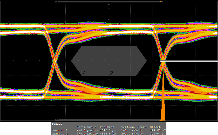
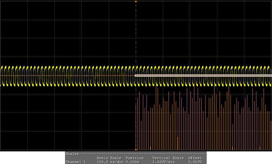 7-9: Clock Jitter
Reference:
Test ID 7-9
7-9: Clock Jitter
Reference:
Test ID 7-9| . | Trial | Actual Value | Margin | HDMIAutomationConfig | Test Frequency(MHz) | # Edges | Tbit(ps) | Clock Jitter(ps) |
| Avg | 30.65 mTbit | 87.80 % | ||||||
| StdDev | 392.4 µTbit | 282.8 m% | ||||||
| Range | 555.0 µTbit | 400.0 m% | ||||||
| Min | 30.37 mTbit | 87.60 % | ||||||
| Max | 30.92 mTbit | 88.00 % | ||||||
| Sum | 61.29 mTbit | 175.6 % | ||||||
| Trial 1 | 30 mTbit | 88.0% | Not defined | 74.178 | 16.000000000 M | 1.348109 k | 40.940 |
| Trial 2 (Worst) | 31 mTbit | 87.6% | Not defined | 74.175 | 16.000000000 M | 1.348169 k | 41.690 |
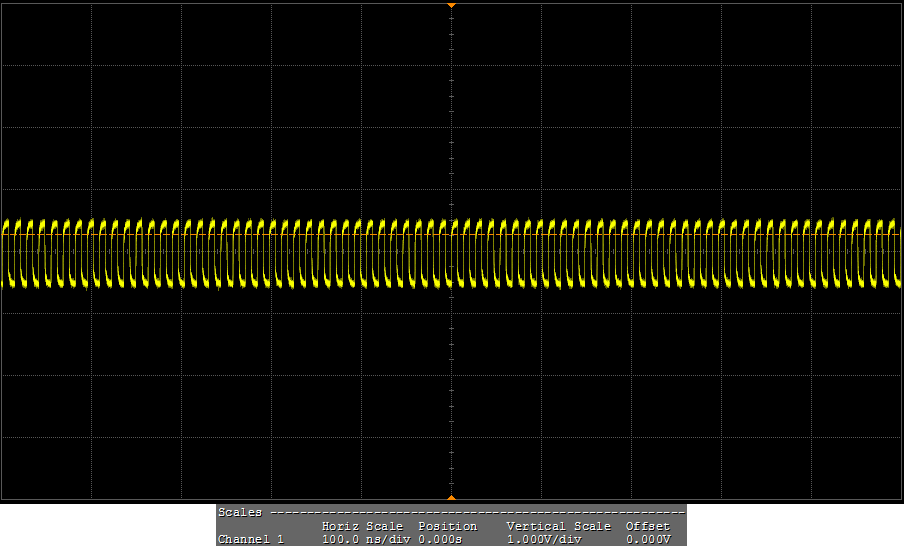
 7-4: Clock Rise Time
Reference:
Test ID 7-4
7-4: Clock Rise Time
Reference:
Test ID 7-4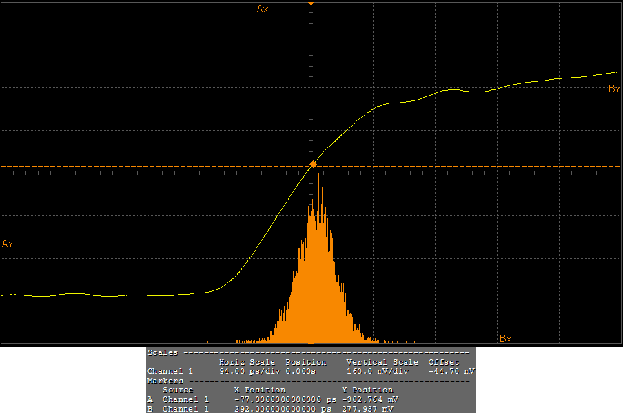 7-4: Clock Fall Time
Reference:
Test ID 7-4
7-4: Clock Fall Time
Reference:
Test ID 7-4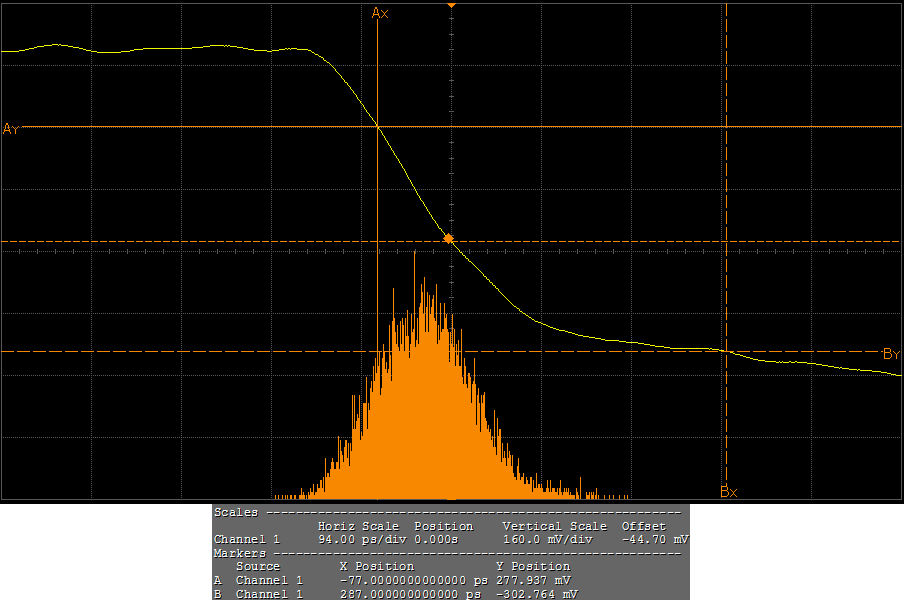 7-8: Clock Duty Cycle(Minimum)
Reference:
Test ID 7-8
7-8: Clock Duty Cycle(Minimum)
Reference:
Test ID 7-8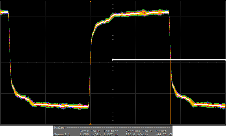 7-8: Clock Duty Cycle(Maximum)
Reference:
Test ID 7-8
7-8: Clock Duty Cycle(Maximum)
Reference:
Test ID 7-8