Engineers must keep abreast of the latest development in PLD designs so they can properly evaluate programmable logic products.
By: Martin Won, Technical Staff Member, Altera Corp.
Contents
• Device Characteristics and Features
• Another Building Block
• Selecting a Scheme
• Design Tools
• Megafunctions for Wireless Design
• QPSK Equalizer
• ECC Methods
Flexibility is key in rapidly changing wireless environment. Standards are evolving daily and customer requirements are changing by the minute. Thus, today's wireless design engineers need products that will let them quickly upgrade or change the functionality of their current products with minimal effort. Programmable logic devices (PLDs) are, therefore, becoming a more integral component in today's wireless system designs.
A number of considerations face the potential user of PLDs. With the rapid change in the capacity, complexity, and feature set of PLDs, it greatly benefits engineers to keep abreast of the latest developments of these devices so that they can correctly evaluate when to use PLDs and which ones to employ
Device Characteristics and Features
In practice, device issues are a key concern when selecting a specific logic product. The size of the design in terms of logical gates, memory bits, and pin count along with the performance characteristics of a specific architecture are the most useful numbers in this respect.
Previous experience with a given device or device family is the best resource for estimating how your design will fit into a PLD. In the absence of this experience, however, PLD vendors generally offer several resources for determining the size of the device that will best fit your design.
Most if not all PLDs are specified with gate count estimates of the total capacity of the device. For example, FLEX 10K devices from Altera are specified with gate counts from 10,000 to 250,000. These gate counts are defined as "typical" gate counts, since different applications use the device resources differently. To reflect this situation, these devices are also specified with a gate count range (from 149,000 to 310,000 gates for the EPF10K250A) and a list of device utilization figures for various functions (Table 1).
Table 1 indicates device resources including logic elements and embedded array blocks. Most are composed of arrays or groups of lower-level building blocks like these. An understanding of the nature of these blocks often gives the designer insight into the implementation PLDs and performance of specific functions in the PLD in question.
For example, in the case of the highest-density devices from the programmable logic industry leaders, such as Altera and Xilinx, the devices are composed of basic building blocks that include a four-input look-up tables, carry chains, and a flip-flop. In the case of the Altera devices, this structure is called a logic element (Figure 1).
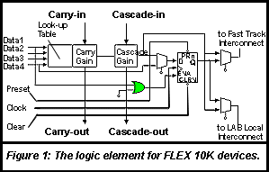
In these PLD devices, four-input look-up tables implement any function of four inputs (four-input AND, OR, NAND, NOR, etc.). Devices with this basic building block have a high flip-flop-to-logic ratio, making them well suited for register-intensive and data processing-type applications.
Most PLD building blocks are a variation on the theme of some amount of combinatorial logic feeding a flip-flop. After the four-input look-up table, the most common involves using product terms feeding an "OR" structure which then connects to one or more flip-flops.
PLDs from Altera, Xilinx, Vantis, Lattice, and others use a structure that has a higher logic-to flip-flop ratio than the logic element. As a result, these types of PLDs are better suited for designs requiring complex controller and state machine-type functions.
Another Building Block
Memory structures are another building block in PLDs. In general, there are two different schemes that PLD vendors use to implement on-board memory in their devices: distributed memory and embedded memory.
Distributed memory, such as that found in Xilinx XC4000 devices, involves the conversion of logic resources into memory resources. On the other hand, embedded memory, like that found in Altera FLEX 10K devices, employs dedicated memory structures, which is generally 2,000 to 4,000 b in size (Note: These embedded structures can be used to implement large look-up table-oriented logic if not used as memory).
Distributed memory tends to be more resource-efficient for small memory structures (much smaller than 2,000 in size). In larger memory structures, however, distributed memory is much slower and uses more resources than embedded memory.
Selecting a Scheme
To aid the user in selecting a type of memory scheme, PLD vendors generally provide resource utilization and performance numbers for various representative memory functions.
For example, the embedded memory structures in FLEX 10K devices (called embedded array blocks [EABs]) can implement random-access memory (RAM) blocks of 2 kb each in several configurations (4 KB each in FLEX 10KE devices). The number of EABs in a FLEX 10K device ranges from 3 to 24. Therefore, a single EAB can be used to build a 256 x 8, 512 x 4, 1024 x 2, or 2048 x 1 RAM in a FLEX 10K device and 256 x 16, 512 x 8, 1024 x 4 or 2048 x 2 RAM in a FLEX 10KE device.
EABs can also be cascaded to build larger memories. As a result, a 4-kb RAM (ie, 256 X 16) could be built with two EABs in a FLEX 10K device while an 8 KB RAM (i.e. 256 x 32) could be built with two EABs in a FLEX 10KE device.
Design Tools
Besides device selection, another important step in using programmable logic is the integration of the PLD design development into your overall design flow. Development tools are the key to accomplishing this integration.
PLDs require development tools to convert of design information into programming data. Often, these tools can be used either exclusively to create, simulate, and program a PLD design, or they can be integrated into a design flow involving other electronic design automation (EDA) tools.
In their stand-alone form, PLD development tools often provide the means to capture a design in some fashion (typically via schematic or behavioral language), place-and-route it into the desired device, and verify its operation either with simulation or with static timing analysis. Most of these tools support industry-standard hardware description languages (HDLs) such as VHDL and Verilog to provide easy interfaces with current wireless designs.
The development tools also use HDLs as a means of linking with other EDA tools. For example, a VHDL design can be created that can be input into a synthesis tool like Synopsys' FPGA Express and also Altera's MAX+PLUS II. In turn, MAX+PLUS II can produce a VHDL or Verilog version of a processed design that contains timing information for use with a system-level simulator.
As a result of this kind of standardization, systems developers who have a well-developed design flow in place can usually integrate a programmable logic design flow into their overall flow with little difficulty.
If a designer plans to use a VHDL or Verilog-based design for both programmable logic and custom application-specific IC (ASIC) development, there are some considerations that result from the architectural differences. These considerations, however, can be handled with some forethought and planning.
For example, since embedded memory structures differ in PLDs and embedded gate arrays, a memory-using design intended for both types of devices can be created in sections (or hierarchically), with two versions of the memory section. The rest of the design can be identical for both the PLD and custom ASIC implementation.
Megafunctions for Wireless Design
Several large functions (or "megafunctions") useful to wireless design have been developed for programmable logic by PLD companies, design groups, and independent designers. These megafunctions range from basic building blocks, such as arithmetic and logical functions, to complex functions for communications such as error correction and control (ECC) and convolutional interleaving.
Megafunctions are attractive to wireless designers because of their flexibility and performance. In fact, some megafunctions can even outperform assignment-specific components designed to run the same function.
The major programmable logic vendors have started partnerships with megafunction developers to improve the quality and use of intellectual property (IP) for programmable logic. For example, Altera founded the Altera Megafunctions Partnership Program (AMPP), which now includes over 25 developers and 100 megafunction offerings. Often, these megafunctions are designed for both programmable logic and ASIC implementations to facilitate a transition to a custom device if necessary. Several are also designed to be configured by the user within the design tools without intervention from the megafunction developer.
KTech Communications has developed a convolutional interleaver megafunction for PCS and other communication systems (Figure 2). This interleaver accepts the input signal 8 b at a time, and at each byte clock cycle, the input and output selector arms shift to the next set of data. When the final index N is reached, the selector arms go back to the initial index 1 arm, and the selector arms continue with each byte cycle. After the latency delay (introduced by the interleaver) passes, the output produces 8 b at a time.
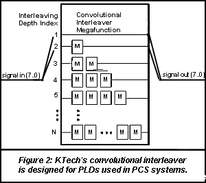
When implemented in a FLEX 10K device, KTech's interleaver uses the on-board memory structures (embedded array blocks) to support interleaving sizes of up to N x M bytes (where N is final index and M is the bit memory stage FIFO shift register size).
QPSK Equalizer
Another programmable logic megafunction available for wireless communications is the quadrature phase-shift keying (QPSK) equalizer from Integrated Silicon Systems, Inc. (Figure 3).
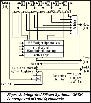
This QPSK equalizer is composed of two channels (I and Q). Each channel has been implemented as a 7-tap finite impulse response (FIR) filter, where the coefficients are updated using the LMS algorithm. All operations perform at the symbol rate, except the coefficient update, which is performed every 12 clock cycles. All the input and output words for the 7-tap LMS FIR filter megafunction are bit-parallel and all the signals are active high. The QPSK equalizer requires 2,500 logic elements (almost 87% of the 50,000-gate EPF10K50) and operates at 61 MHz in the fastest speed grade of the device.
ECC Methods
The proliferation of digital technology in wireless designs has increased the demand for error control coding (ECC) methods. One of the most popular ECC methods for wireless communication systems is the Reed-Solomon (RS) code.
Several megafunctions for RS encoder and decoder functions are available for programmable logic. Performance and resource utilization varies based on codeword length N and number of check symbols R. Table 2 lists some representative figures for several configurations of encoders and decoders from HammerCores.
|
|
|
|
|
|
|
|
|
|
|
|
|
|
|
|
|
|
|
|
|
|
|
|
|
|
|
|
|
|
|
|
|
|
|
To facilitate the customization of these functions, HammerCores has developed a MegaWizard to allow users to change the implementation parameters within a PLD tool. Using the MegaWizard, users set the total number of symbols, number of check symbols, bits per symbol, field value, and the first root, as well as other parameters.
Several other megafunctions of interest to wireless systems designers are available, including convolutional encoders, digital modulators, and data rate framers/deframers. The number and type of functions that are being developed for communications-oriented designs is constantly on the increase. A good way to research the availability of a given function is to contact a programmable logic vendor.
About the author…
Martin Won, Technical Staff Member, Altera Corp., 101 Innovation Drive, San Jose, CA 95134. Phone: 408-894-7000; Fax: 408-544-6411.