by Bing Fong Ma
Introduction
Step-up or boost DC/DC converters traditionally suffer from a lack of
true shutdown capability. The output of a boost converter is connected to
the input through the inductor and diode, so when the device is powered
down the load is still connected to the input source, presenting a possible
discharge path. Even some synchronous boost converters suffer from this
limitation. The unique configuration of the LT1306's internal 2 ampere
switch and rectifier overcomes this limitation. When the LT1306 is shut
down, the output is disconnected from the input, eliminating the discharge path.
Additionally, the LT1306 can regulate the output when the input
voltage exceeds the output voltage. This is useful for generating a 5V
supply from a 4-cell alkaline battery. When fresh, the battery voltage
measures about 6.5V, but when depleted, the battery voltage is only 4V. A
simple boost converter output will follow the input voltage when the
battery voltage exceeds 5V, while a step-down, or buck converter will lose
regulation when the battery voltage falls below 5V. The LT1306 regulates the
output to 5V in both situations.
Lastly, the LT1306 controls inrush current. A user installing a new
battery need not worry about high inrush current as the battery initially
charges the output capacitor. The LT1306 provides a clean solution to a
difficult problem.
The LT1306 packs all these features in an SO-8 package.
The constant frequency, current mode PWM device runs at 340kHz and
features Burst ModeTM operation to maintain high efficiency at light
loads. No-load quiescent current is 160µA, while the device consumes just
9µA in shutdown. The device can be externally synchronized to
frequencies between 425kHz and 500kHz.
In the block diagram of Figure 1, the PWM control path is shown
enclosed within the dashed line. The free-running frequency of the oscillator
is trimmed to 340kHz. The main power switch, Q1, is turned on at the
trailing edge of the clock pulse. Q1 is switched off when the switch
current (sensed across resistor RS) exceeds
a programmed level set by the error amplifier output
,VC, and the compensation ramp. This is current
mode control. The switch current limit is reached when
VC clamps at 1.28V.
Circuit Description

Figure 1. LT1306 block diagram
The error amplifier output determines the peak switch
current required to regulate the output voltage.
VC is therefore a measure of the output power. At heavy loads,
the peak and average inductor current are both high. The LT1306
operates in continuous-conduction mode (CCM). As the load decreases, the average
inductor current moves lower with an accompanying decrease in the peak
inductor current. If the inductor current returns to zero within each
switching cycle, the converter is said to operate in discontinuous-conduction
mode (DCM). Further reduction in load moves
VC towards its lower operating range.
Hysteretic comparator A3 determines if
VC is too low for the LT1306 to operate efficiently. As
VC falls below the Burst Mode threshold,
VB, comparator A3 turns off Q1. Any
energy stored in the inductor is delivered to the output through the
synchronous rectifier. The LT1306 draws only 160µA from the input in this
idle state. As the output voltage droops,
VC rises above the upper trip point of A3. The LT1306 again wakes up
and delivers power to the load. If the load remains light, the output voltage
will rise and VC will fall, causing the
converter to idle again. Power delivery therefore occurs in bursts. The
burst frequency is dependent on the input voltage, the inductance, the load
current and the output filter capacitance. The output voltage ripple in
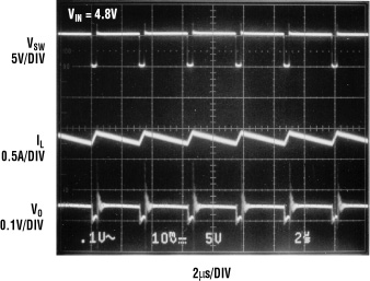
Burst Mode operation is higher than those in CCM and DCM operation.
Burst operation increases light load efficiency because the higher peak
switch current characteristic of Burst Mode operation allows the converter to
deliver more energy in each switching cycle than possible with
cycle-skipping DCM operation. Thus, fewer switching cycles are required to
maintain a given output. Chip supply current also becomes a small fraction
of the total input current.
The synchronous rectifier is represented as an NPN transistor, Q2,
in the block diagram. A rectifier driver, X5, supplies variable base drive to
Q2 and controls the voltage across the rectifier. The supply voltage for
driver X5 is generated locally with the bootstrap circuit comprising D1 and
C1. When switch Q1 is on, the bootstrap capacitor C1 is charged from the
input to the voltage
VIN–VD1(ON)
– VCESAT1. The charging current
flows from the input through D1, C1 and Q1 to ground. After Q1 is
switched off, the node SW goes above VO by
the collector–emitter saturation voltage of Q2. D1 becomes reverse biased
and the CAP pin voltage is approximately
VO + VIN – VD1(ON). Capacitor C1
supplies Q2's base drive. The charge consumed is replenished during
Q1's on-interval.
In boost operation, X5 drives rectifier Q2 into saturation with
constant forced b. X5 ceases supplying base current to Q2 when the
inductor current falls to zero. If VIN is
greater than VO, Q2 will not be driven
into saturation. Instead, the collector–emitter voltage of Q2 increases
so that the inductor voltage reverses polarity as Q1 switches. Since
the inductor voltage is always bipolar, volt-second balance can be
maintained regardless of the input voltage. The LT1306 can therefore operate
as a step-down converter.
During start-up, the inductor voltage of a boost converter with a
diode rectifier remains positive until the output voltage rises to one diode
voltage below the input voltage. A high input-transient current spike
invariably results. In the LT1306, the inductor voltage reverses polarity every switching cycle. This, with cycle-by-cycle current limit,
eliminates the inrush current spike.
The rectifier voltage drop depends on both the input and output
voltages. Efficiency in step-down operation is approximately that of a linear
regulator. For sustained step-down operation, the maximum output
current will be limited by the package thermal characteristics.
A hysteretic comparator inside driver X5, which detects the
crossover between the input and the output voltages, signals the driver to
provide appropriate base current to the rectifier. DC transfer characteristics
of this comparator are illustrated in Figures 2 and 3.