by Brian Hamilton
Introduction
The LT1395, LT1396 and LT1397 are 400MHz current feedback
amplifiers with a high slew rate and a –3dB bandwidth that remains
relatively constant over a wide range of closed-loop gains. The current
feedback topology of the LT1395/LT1396/LT1397 family can provide
improved performance in many new and existing designs that have historically
used voltage feedback op amps. Because of its current feedback topology,
the LT1395/LT1396/LT1397 family boasts a slew rate of 800V/µs on
a supply current of only 4.6mA per amplifier, resulting in a much
higher full-power bandwidth than comparable voltage feedback op amps.
The current feedback topology of the LT1395/LT1396/LT1397 also
results in additional design flexibility because the –3dB bandwidth remains
relatively constant regardless of closed-loop gain. In contrast, the –3dB
bandwidth of voltage feedback op amps decreases in proportion to the
closed-loop gain that has been chosen. For example, a voltage feedback op
amp with a 400MHz gain bandwidth product (GBW) will only have a
100MHz bandwidth at a closed-loop gain of four. At the same gain, the LT1395/LT1396/LT1397 have a gain bandwidth of approximately 240MHz. The
parts have industry-standard single,
dual and quad pinouts allowing easy upgrades of existing applications.
The LT1395/LT1396/LT1397 Family
In addition to a 400MHz –3dB bandwidth and an 800V/µs slew rate,
the LT1395/LT1396/LT1397 family has exceptionally flat frequency
response. Applications that require gain accuracy across a broad frequency
range will benefit from the family's ±0.1dB bandwidth, which exceeds
100MHz. For increased design flexibility, the LT1395/LT1396/LT1397 also
boast a very flexible output stage. They have over 80mA of output current
drive, and on ±5V supplies they can swing up to ±3.6V with a 150W load.
The LT1395/LT1396/LT1397 family's wide supply voltage
range and versatile packaging options also increase design flexibility.
Supplies can range from a single 4V to ±6V.
All devices and package types are compatible with standard op amp
pinouts. In addition to standard SO packages, the LT1396 and LT1397 are also
available in smaller form factors. The LT1396 is available in an 8-lead
MSOP package. The LT1397 is available in a 16-lead SSOP package that takes
the same amount of board space as an SO-8. The LT1395 will be available
in SOT-23 soon.
A simplified schematic of a single amplifier from the
LT1395/LT1396/LT1397 family can be seen in Figure 1. Transistors Q1–Q7, J1 and
R1 generate the necessary internal bias currents, with Q6 and Q7 acting
as current sources for the input stage. Transistors Q8–Q11 form the
amplifier's input stage. Currents coming from Q10 and Q11 are mirrored
on top and bottom by transistors Q12–Q17. The collectors of transistors
Q13 and Q15 drive the high impedance node of the amplifier. Transistors
Q16 and Q17 act as current sources for the output stage. Transistors
Q18–Q21 and resistors R2 and R3 form the output stage.

Figure 1. LT1395/LT1396/LT1397 simplified schematic (one amplifier)
It's the Input Stage
The advantages of a current feedback amplifier (CFA) can be better
understood by examining the internal circuit topology in greater detail.
The LT1395/LT1396/LT1397 input stage reveals that the noninverting
input drives the bases of Q8 and Q9, resulting in a high impedance input. On
the other hand, the inverting input drives the emitters of Q10 and Q11
and results in a low impedance input; any differential voltage imposed
across the inputs creates a current that flows into or out of the inverting input.
This current modulates the collector currents of Q10 and Q11, is mirrored
on top and on the bottom, and produces a voltage swing at the
high-impedance node (and output) of the amplifier. Since the output
voltage swing is based upon the current flowing through the inverting input,
the gain of a current feedback amplifier is expressed as the ratio of output
voltage change (dV) divided by inverting input current change
(dIB–), and is referred to as the amplifier's
transimpedance (Z0).
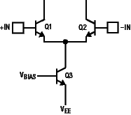
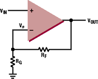
A conventional voltage feedback input stage (Figure 2) is
dramatically different than the current feedback input stage described above.
The inverting input of the voltage feedback input stage is a high
impedance input; thus, any feedback to this node is in the form of a voltage. Since
the currents flowing into or out of the inverting input are small,
the maximum slew current at the high-impedance node is derived
from internal currents only and has an upper limit equal to the collector
current of Q3. In contrast, the slew current in a CFA is not limited
to internal currents; it is provided externally via the inverting input
and results in much higher slew rates than those of conventional
voltage feedback op amps.