by Doug La Porte
No More Complex Equations, No More Precision
Capacitors, No More Frustration
The LTC1563-2 and LTC1563-3 form a family of extremely easy to use, 4th order active RC lowpass filters (no signal sampling or clock requirements). They cover cutoff frequencies ranging from 256Hz to 256kHz while operating at supplies from as low as a single 3V (2.7V minimum) up to ±5V. The LTC1563 also features rail-to-rail input and output operation with, typically, 1mV of DC offset. The design of the most popular filter responses is trivial, requiring only six resistors of identical value and no external capacitors. The cutoff frequency of unity-gain Butterworth or Bessel filters is set with a single resistor value calculated using the following simple formula:
R = 10kW • (256kHz/fC)
where fC is the cutoff frequency in Hertz.
The LTC1563-2 is used for a Butterworth response, whereas the LTC1563-3 is used for a Bessel response.
Beyond design simplicity, the LTC1563 facilitates manufacturability. For a discrete design to achieve the ±2% cutoff frequency accuracy of the LTC1563, precision capacitors (2% or better) are required. These capacitors are not readily available and can present a difficult and costly purchasing problem. A typical discrete design also requires four resistor values and four capacitor values—eight reels of components. This leads to eight times the purchasing, stocking and assembly costs and eight reels of components on the automated assembly machine. Many large circuit boards require more component reels than the assembly machine can accommodate leading to costly secondary operations. The LTC1563 decreases purchasing, stocking and assembly costs while removing seven component reels from the assembler.
The LTC1563 is also very versatile. The proprietary architecture yields effortless design of the unity gain Butterworth and Bessel filter responses while still allowing complex, arbitrary filter responses with any gain desired. A Chebyshev, Gaussian or any other all-pole response, with or without gain, can be obtained using unequal valued resistors calculated with a more complex set of equations (for the best results use FilterCAD version 3.0). Designs ranging from a dual 2nd order filter up to an 8th order filter (two cascaded devices) are also easily obtained. With the addition of two capacitors, a single LTC1563 can be used to implement a 6th order lowpass filter. In another application, the two additional capacitors render a simple wideband, low Q bandpass filter.
Salient performance features of the LTC1563 family include the following:
256Hz < fC < 256kHz
fC accuracy < ±2% (typ)
Continuous time filter—no clock, no sampling
SINAD 95dB at 3VP-P, 50kHz—compatible with 16-bit systems
Rail-to-rail input and output operation
Output DC offset voltage < ±1mV (typ)
DC offset drift < ±5µV/°C (typ)
Operates from a single 3V (2.7V min) to ±5V supplies
Low power mode, ISUPPLY = 1mA (typ), fC < 25.6kHz
High speed mode, ISUPPLY = 10mA (typ), fC < 256kHz
Shutdown mode, ISUPPLY = 1µA (typ)
Narrow SSOP-16 package, SO-8 footprint
Typical 4th Order Butterworth and Bessel Applications
Figure 1 illustrates a typical LTC1563 single-supply application, with
Figure 2 showing the Butterworth frequency response of the
LTC1563-2 and Figure 3 showing the Bessel frequency response of the
LTC1563-3. As the R value is decreased from 10M to 10k, the cutoff frequency
increases from 256Hz to 256kHz. For cutoff frequencies below 25.6kHz,
significant power can be saved by placing the LTC1563 into the low power
mode. Connect the *LP pin to the V–
potential to enable the low power mode. All other applications should place
the part in the high speed mode by leaving the *LP pin open or connecting it
to the V+ potential. The high speed
mode, in addition to supporting higher cutoff frequencies, has a lower DC
offset voltage and better output drive capability than the low power mode.
The minimum supply voltage in the high speed mode is 3V, whereas the
low power mode supports 2.7V operation. The shutdown mode is
available at all times. The *EN pin is internally pulled up to the
V+ potential, causing the LTC1563 to default to the
shutdown mode. To enable normal operation, the *EN pin must be
pulled to ground. In the shutdown mode, the supply current is typically 1µA
and 20µA maximum over temperature.

Figure 1. Typical LTC1563-X single-supply application |
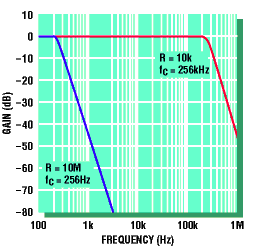
Figure 2. LTC1563-2 Butterworth response of Figure 1's circuit for
|
Figure 2. LTC1563-3 Bessel response of Figure 1's circuit for
|
Performance SpecificationsLTC1563 family has outstanding DC specifications. The DC offset of the filter in the high speed mode is typically ±1mV, with a maximum offset over temperature of ±3mV. The DC offset is slightly greater in the low power mode at ±5mV maximum over temperature on the lower supply voltages and ±6mV maximum over temperature on a ±5V supply. The DC offset drift is only 5µV/°C. |
The LTC1563's SINAD performance with lower signals is dominated
by the noise of the part. Figure 4 is a plot of the noise vs the cutoff
frequency. The total integrated noise (over a bandwidth of twice the cutoff frequency)
is 32µVRMS at the lowest cutoff
frequency and increases to 56µVRMS at the
highest cutoff frequency. Figure 5 shows the SINAD performance as
function of the input signal amplitude for a 50kHz signal. The plot
demonstrates that distortion is not a significant factor at smaller signal
amplitudes. Distortion is only noticeable when the signal amplitude is very
large, within about 1V of the supply rails. The distortion performance also
holds up well at higher frequencies, as Figure 6 illustrates. The SINAD is
nearly flat over all frequencies, indicating again that noise is the
determining function. The SINAD is about 95dB for the
3VP-P input, indicating that this part is very suitable for
16-bit systems.

Figure 4. LTC1563-X total integrated noise vs cutoff frequency |

Figure 5. LTC1563-X THD plus noise performance vs signal amplitude |

Figure 6. LTC1563-X THD plus noise vs signal frequency |
Transfer Function Capabilities
The LTC1563 was designed to make implementing standard
unity-gain, 4th order Butterworth and Bessel filters as simple as possible.
Although this goal was accomplished, the part also maintains tremendous
flexibility. Virtually any all-pole transfer
function can be realized with the LTC1563-2. Table 1 lists the many filter
configurations attainable with the LTC1563 family. The actual transfer
function (pole locations) of the filter is nearly arbitrary.
| Design | LTC1563 Support | FCAD 3.0 Support |
|---|---|---|
| 2nd order LPF | Yes | Yes |
| Dual 2nd order LPF | Yes | Yes |
| 3rd order LPF (one capacitor) | Yes | Yes |
| Dual 3rd order LPF (two capacitors) | Yes | Yes |
| 4th order LPF | Yes | Yes |
| 5th order LPF (one capacitor) | Yes | Yes |
| Pseudo–6th order LPF (one part, two capacitors) | Yes | Yes |
| Standard 6th order LPF (two parts, no capacitors) | Yes | Yes |
| 7th order LPF (one capacitor) | Yes | Yes |
| 8th order LPF | Yes | Yes |
| 9th order LPF (one capacitor) | Yes | Yes |
| Wideband bandpass (two capacitors) | Yes | No |
4th Order Lowpass Filters with Gain
Filters responses other than Butterworth and Bessel, filters with gain and higher order filters are easily obtained with the LTC1563. The design equations are more complex than the simple unity-gain Butterworth and Bessel equation. Refer to the LTC1563 data sheet for the actual equations. For the best design result, use FilterCAD version 3.0 (or later). FilterCAD uses a very complex and accurate algorithm to account for most parasitics and op amp limitations. Using FilterCAD will yield the best possible design.
Figure 7 shows an LTC1563-2 employed to make a 4th
order, 150kHz, 0.5dB ripple Chebyshev lowpass filter with a DC gain of 10dB.
The frequency response is shown in Figure 8. All of the gain is realized in
the first section to achieve the lowest output voltage noise. Note that
the schematic, and thus the PC board layout, is the same as a unity
gain Butterworth lowpass filter except that the resistor values are different.
The same PC board layout could be used to build an infinite number of
lowpass filters, each with a different gain, transfer function and
cutoff frequency.

Figure 7. 0.5dB, 150kHz Chebyshev lowpass filter with a DC gain of 10dB |

Figure 8. Frequency response of Figure 7's circuit |
8th Order Lowpass Filter
Designing an 8th order filter is just as easy as a 4th order filter. Of
course, the final solution uses twice as many components but the design is
essentially the same procedure. Using FilterCAD makes the design
procedure simple and straightforward. Figure 9a shows the schematic for
a 180kHz 8th order, Butterworth lowpass filter with a gain of 6dB
and Figure 9b is a plot of its frequency response. The solution is quite compact,
simple to layout on the PC board and uses only standard 1% resistors. A
discrete solution would involve several precision capacitors and a much
more complicated layout accompanied by numerous layout-related
parasitics. With the discrete solution, you may not get the response that you
expect, due to these parasitic elements.
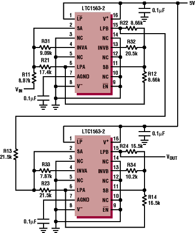
Figure 9a. 180kHz 8th order, Butterworth lowpass filter with a DC gain of 6dB

Figure 9b. Frequency response of Figure 9a's circuit |
Pseudo–6th Order Lowpass FilterA textbook, theoretical 6th order lowpass filter is composed of three 2nd order sections, each realizing a complex pole pair. The LTC1563 has two 2nd order sections to yield two complex pole pairs. A 6th order lowpass filter can be made using two LTC1563 parts (with half of the second part unused) or, by using an old filter trick, it can be implemented with a single part. |
First a little background material (a bit of filter theory, but not too
bad). Each 2nd order, complex pole pair can be defined by the parameters
fO and Q. Figure 10 illustrates that
each complex pole pair has the same real component and the
complementary imaginary components. The
fO parameter is the magnitude of the poles and the Q is a measure of
how close the poles are to the real or imaginary axis. The closer the
poles are to the imaginary axis, the higher the Q becomes, until Q reaches
infinity when the poles are directly on the imaginary axis. As the pole pair
moves close to the real axis, the Q decreases in value until the Q is at 0.5
when they are both on the real axis. A pole pair with a Q of 0.5 is
mathematically identical to two 1st order, real poles.

Figure 10. Locations of complex pole pairs of fixed fO and different Qs |

Figure 11. Pole locations for classic Butterworth and pseudo-Butterworth lowpass filters |
Armed with a little filter knowledge, we are now ready for the trick. All 6th order filters have three fO and Q pole pairs. The pair with the lowest Q usually has a Q somewhere between 0.5 and 0.6. The trick is to substitute two 1st order, real poles (the equivalent of a 2nd order section with a Q of 0.5) for the pole pair with the lowest Q value. To compensate for this bending of the ideal mathematics, it is necessary to go back and tweak some or all of the fO and Q values in the design. The resulting filter is no longer the exact, ideal, theoretical mathematical implementation, but with care you can get a frequency response and a step response that differ imperceptibly from the textbook plots. The name "pseudo–6th order filter" is somewhat misleading, because the filter is clearly of the 6th order (six poles with a final attenuation slope of –36dB/octave). It is only "pseudo" in the sense that the filter does not conform to the classical, standard mathematical models. If your company is shipping mathematics, stick with the textbook 6th order response. However, realize that once you consider the component tolerances, you still end up with an approximation. Most products really require filters that meet a specific set of performance criteria (for example, cutoff frequency, passband flatness, stopband attenuation, step response overshoot and step response settling) in a simple, reproducible and cost effective manner. The textbook responses are just a convenient way to synthesize a filter (or a good starting point in the filter design).
The classical response is tweaked manually using the FilterCAD Custom Design feature. Start with the textbook 6th order lowpass filter. Open the Step Response and Frequency Response windows by clicking on the appropriate buttons. In each response window, save the trace to compare the responses with the tweaked design. Next, click on the Custom Response button, remove the low Q section and add two 1st order lowpass sections at the same fO. Finally, alter the new design's fO and Q parameters as required, while monitoring the frequency and step response windows, until the desired responses are achieved. With some practice, an intuitive sense of which parameters need adjustment is developed.
The procedure is clearly illustrated with the following 6th order
100kHz Butterworth lowpass filter example. Figure 11 shows the pole
locations and fO and Q values for a textbook
6th order Butterworth lowpass filter and the pseudo–6th order equivalent
values. The circuit implementation, Figure 12, of this transfer
function uses a standard 4th order type of circuit where the input resistor
is split into two resistors with an additional capacitor to ground in
between the resistors. This "TEE"
network forms a single real pole. By making this modification to both sections,
a pair of real poles is added to the 4th order network forming the
desired pseudo–6th order filter. The TEE network technique is also used to
give the single real pole required in all odd-order responses.

Figure 12. 100kHz, 6th order pseudo-Butterworth lowpass filter
Wideband Bandpass Filters
Although the LTC1563 family does not directly support classical bandpass filters, you can successfully implement a wideband bandpass filter using the standard 4th order lowpass circuit and a couple of additional capacitors. The resulting filter is more of a highpass-lowpass type of filter than a true bandpass. You can design outstanding, highly selective bandpass filters using the LTC1562 family of universal filter products (see Linear Technology VIII:1 [February 1998] and IX:1 [February 1999])—the best continuous time filters in the industry for bandpass and elliptic highpass or lowpass filters. Although the LTC1562 is the best part for narrowband bandpass filters, if your requirements are less stringent, the LTC1563 family can provide a simple, cost-effective wideband bandpass filter.
Figure 13 shows the schematic of an LTC1563-3 used to make a simple, wideband bandpass filter centered at 50kHz. The frequency response is shown in Figure 14. The design procedure for this type of filter does not conform to any standard procedure. It is best to start with a standard lowpass filter and add two 1st order highpass sections to the transfer function. Adjust the highpass corner and the lowpass fC up and down until the desired transfer function is achieved. The design in Figure 13 starts with a standard, unity gain, 4th order Bessel lowpass filter with a cutoff frequency of 128kHz. Each section is then AC coupled through the 680pF capacitors. Each capacitor, working against its input resistor, realizes a 1st order highpass function with the cutoff frequency (11.7kHz in this design) defined by the following equation:
fC = 1/(2 • p • R • C) (R = R11 or R12)

Figure 13. 50kHz wideband bandpass filter |

Figure 14. Frequency response of Figure 13's circuit |
The resulting circuit yields a wideband bandpass filter that uses only one resistor value and one capacitor value. Note that although FilterCAD does not provide complete support for this type of filter with the LTC1563, you can still use the program's Custom Design mode to set the required transfer function. After the transfer function has been chosen, use FilterCAD to design the lowpass part of the filter and then use the simple highpass formula above to complete the circuit.
Driving 16-Bit ADCs
The LTC1563 is suitable for 16-bit systems. Figures 3 through 5 show that the LTC1563's noise and SINAD is commensurate with 16-bit data acquisition systems. These measurements were taken using laboratory equipment and well-behaved loading circuitry. Many circuits will perform well in this environment only to fall apart when driving the actual A/D converter. Many modern ADCs have a switched capacitor input stage that often proves to be difficult to drive while still maintaining the converter's 16-bit performance. The LTC1563 succeeds with only a little help from a resistor and a capacitor.
Figure 15 shows the LTC1563-2 configured as a 5th order,
22kHz, 0.1dB ripple Chebyshev lowpass filter driving an LTC1604 16-bit
ADC. The converter operates with a 292.6kHz sample clock. The
22kHz Chebyshev filter has attenuation of about 96dB at the Nyquist
frequency. This is a very conservative antialiasing filter that guarantees aliasing
will not occur even with strong input signals beyond the Nyquist frequency.

Figure 15. 0.1dB, 5th order, 22kHz Chebyshev lowpass filter driving an LTC1604 16-bit ADC
|
Figure 16 shows a 4096 point FFT of the converter's output while being driven by the LTC1563 at 20kHz. The FFT plot shows the fundamental 20kHz signal and the presence of some harmonics. The THD is –91.5dB and is dominated by the second harmonic at –92dB. The remaining harmonics are all well below the –100dB level. There are also some nonharmonically related spurs that are artifacts of the ADC. In the filter's passband, the noise level is slightly higher than the converter's. The peaking of the noise level at the cutoff frequency, mostly due to the high Q section, is a typical active filter characteristic. In the stopband, the noise level is essentially that of the converter. The end result is a SINAD Figure of 85dB, about 4dB less than the converter alone. |

Figure 16. FFT of the ADC output data from Figure 15's circuit |
Conclusion
The LTC1563 continuous time, active RC lowpass filter is an
economical, simple to use, yet versatile part that meets the high performance
standards required in today's high resolution systems. Beyond ease
of use, the part's design simplicity leads to ease of manufacture. This
combination of features makes discrete lowpass filters and expensive,
bulky filter modules obsolete. ![]()