LTC1642: a Hot Swap Controller with Foldback Current Limiting and Overvoltage Protection |
by Pat MaddenHot Circuit InsertionWhen a circuit board is inserted into a "hot" (powered) backplane, its
supply bypass capacitors can draw large currents from the backplane
power bus as they charge. These currents can cause glitches on the
backplane supply voltage, resetting other boards in the system, and can even
destroy edge connectors. Like other members of Linear Technology's Hot
SwapTM family, the LTC1642 limits the charging current drawn by a
board's capacitors, allowing safe circuit board insertion into a hot backplane. It
also offers additional capabilities, some new to the Hot Swap family: a
maximum recommended operating voltage of 16.5V, a programmable
electronic circuit breaker with foldback current limiting, overvoltage protection to
33V, and a voltage reference and uncommitted comparator.
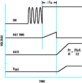
Figure 1. LTC1642 typical Hot Swap applicationIn the circuit shown in Figure 1, the LTC1642 and the external NMOS pass transistor Q1 work together to limit the charging current when a board is plugged into a hot backplane. In this application, the backplane voltage is 12V, but the chip will operate with any supply voltage between 3.0V and 16.5V. When power is first applied to VCC, the chip holds Q1's gate at ground. After a programmable debounce delay, an internal 25µA current source begins to charge the external capacitor C2, generating a voltage ramp of 25µA/C2 V/s at the GATE pin. Because Q1 acts as a source follower while its gate ramps, the current charging the board's bypass capacitance, CLOAD, is limited to 25µA • CLOAD/C2. An internal charge pump supplies the 25µA gate current, ensuring sufficient gate drive to Q1. Resistor R3 protects against high frequency FET oscillations; capacitor C1 sets the debounce delay, DTD, before the GATE pin voltage begins ramping: DTD(ms) = 615• C1(µF). The ON pin is the chip's control input; when it is below 1.22V, the GATE pin is held at ground. If ON/OFF control of the LTC1642 is not required, ON should be tied to VCC through a 51k current limiting resistor. Typical waveforms at card insertion are shown in Figure 2. |
Short-Circuit ProtectionA short circuit from Q1's source to ground can destroy the FET; it can also reset every other card in the system if the backplane supply voltage droops due to the excessive current. The LTC1642 can protect against both threats by limiting the current drawn from the backplane supply during a short circuit and by opening an electronic circuit breaker before Q1 overheats. The addition of analog current limiting to the standard electronic circuit breaker function can improve system performance. For example, consider a system of plug-in cards powered by a backplane supply. The sudden removal of one card causes the backplane voltage to ring at a fairly high frequency, due to the step change in supply current. This ringing signal appears differentially across the sense resistor on each remaining card. It can trip the circuit breaker, even though there is no fault on the card. To prevent this, the designer may attempt to slow the circuit breaker by connecting a lowpass RC network across the sense resistor, only to find that one problem has been exchanged for another: if there is a short circuit on the card, the backplane voltage droops too much before the circuit breaker opens. The LTC1642 shines in this application. It regulates the load current within a few microseconds after a short circuit, before the backplane can droop, but can delay opening the circuit breaker for milliseconds or more, which allows the ringing to decay, resulting in almost complete immunity from backplane noise. |
Figure 2. Typical waveforms at card insertion |
|
The external components that provide short-circuit protection are included in Figure 1. R2 senses the load current, and, if its voltage drop reaches an internal threshold, the current-limit servo loop adjusts the GATE pin voltage such that Q1 acts as a constant current source. R2's voltage limit decreases as the output voltage decreases; this "foldback" tends to keep Q1's power dissipation constant in current limit. The output voltage is sensed at the FB pin. When FB is grounded, the internal threshold voltage is 20mV, but this increases gradually to 50mV with increasing voltage at FB. To compensate this servo loop R4 is added in series with C2; to ensure stability, the product 1/(2 • p • R4 • C2) should be kept below the loop's unity-gain frequency of 125kHz and C2 should be larger than Q1's input capacitance, CISS. The values shown in Figure 1, C2 = 0.047µF and R4 = 330W, work well with the Fairchild FDS6630A and similar MOSFETs. The *FAULT output, when asserted, signals that the circuit breaker has opened. Capacitor C3 and resistor R5 set the delay, DTBRK, between the onset of current limiting and the circuit breaker opening: DTBRK(ms) = [62 R5(kW)] • C3(µF). R5 slows C3's discharge, ensuring that the circuit breaker eventually opens in the event of repetitive, but short, current faults. These are dangerous because the slow voltage ramp at Q1's gate means that it continues to dissipate substantial power for some time after the current limit clears. Larger values of R5 protect against lower duty cycle shorts, at the cost of greater uncertainty in the circuit breaker delay time. A prudent upper limit on R5 is 30k, which will open the circuit breaker if the duty cycle of a repetitive short exceeds 50%. |
|
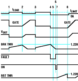
Typical waveforms during a short circuit are shown in Figure 3. The load is shorted to ground at time 1. The GATE voltage drops until Q1 comes into regulation and the circuit breaker timer (BRK TMR) starts. The short is cleared at time 2, before the breaker opens, and the GATE voltage ramps back up. At time 3, the load is shorted again and at time 4 the breaker opens, pulling the GATE to ground and asserting *FAULT. Although the short is cleared at time 5, *FAULT doesn't go high until time 6 (it has an internal 10µA pull-up), after the ON pin has been low for two microseconds. At time 7, ON goes high and the debounce timer (RST TMR) starts; at time 8 the GATE voltage begins ramping. |
Figure 3. Current-limit and circuit-breaker timing |
Powering Up In Current LimitRamping the GATE pin voltage indirectly limits the charging current to I = 25µA• CLOAD/C2, where C2 is the external capacitor connected to the GATE and CLOAD is the load capacitance. If the value of CLOAD is uncertain, a worst-case design can result in needlessly long ramp times, and it may be better to limit the charging current directly by allowing the LTC1642 to power up in current limit. This is perfectly acceptable as long as the circuit breaker delay is long enough to power up under worst-case conditions. |
Automatically Restarting after the Circuit Breaker OpensThe LTC1642 will automatically attempt to restart itself after the
circuit breaker opens if the *FAULT output is tied to the ON pin input. The
resulting waveforms during a short circuit are shown in Figure 4. As the
figure shows, pass transistor Q1's duty cycle is equal to the circuit breaker
delay, DTBRK, divided by the sum of the circuit breaker and debounce delays, DTBRK + DTD. Q1
dissipates substantial power while acting as a constant current source, so
be sure its maximum junction temperature is not exceeded
in worstcase conditions. For example, the FDS6630A in Figure 1
dissipates 24W(= 2A • 12V) DC when the load
is shorted to ground. Its absolute maximum junction temperature,
TJ, is 150°C, so an ambient
temperature, TA, of 85°C requires an effective
junction-to-ambient thermal resistance of 2.7°C/W |
Figure 4. Automatic restart following a short circuit |
Figure A. Fairchild FDS6630A transient thermal response curve (reproduced by permission, from the FDS6630A data sheet)If *FAULT is tied to ON, open-drain logic should be used to drive
the node, and the external pull up resistor at the ON pin may be
omitted, because *FAULT provides a weak internal pull-up.
The LTC1642 can protect a card from excessive voltage by quickly
turning off the pass transistor if the supply voltage exceeds a programmable
limit and by triggering a crowbar SCR after a programmable delay. The
LTC1642 includes an internal regulator that protects against supply voltages
up to 33V. It can also be configured to automatically restart when an
overvoltage condition clears.
The external components that provide overvoltage protection
are included in Figure 1. Resistors R6 and R7 set the overvoltage limit,
timing capacitor C4 sets the delay before the crowbar SCR Q3 fires and
NPN follower Q2 boosts the trigger current into Q3. When
VCC exceeds (1 + R6/R7) • 1.22V, an internal
comparator trips and the chip cuts off Q1 by pulling its gate to ground. For
better noise rejection, the propagation delay through the comparator (on a
low-to-high transition at OV) increases from 20µs to 80µs as the differential
input voltage decreases from 175mV to 3mV. Once the comparator trips, an
internal 45µA current starts charging C4; when it reaches 0.41V the
current increases to 1.5mA and Q2 quickly triggers the SCR. The delay,
DTSCR, before the SCR triggers is
DTSCR(ms) = 9 • C4(µF). Once C4 reaches
0.41V, the LTC1642 latches off. After the overvoltage clears, GATE and
*FAULT remain at ground and the 1.5mA charging current persists. To
restart after the overvoltage clears, hold the ON pin low for at least 2µs and
then bring it high. The GATE voltage will begin ramping up after a
debounce delay. The chip will restart if *FAULT and ON are connected together:
the GATE voltage begins ramping up one debounce delay after the
overvoltage clears.
|
Figure 5. Overvoltage timing |
Figure 5 shows typical waveforms. The OV comparator goes high at time 1, causing the chip to pull the GATE pin to ground and start charging C4. At time 2, before the capacitor reaches 0.41V, OV falls below 1.22V; C4 discharges and the GATE voltage begins ramping after the debounce delay ends at time 3. Another overvoltage begins at time 4, and at time 5 C4 reaches 0.41V; *FAULT goes low and the charging current increases to 1.5mA. Even after OV falls below 1.22V at time 6, GATE and *FAULT stay low and CRWBR continues to source 1.5mA. *FAULT goes high when ON goes low momentarily at time 7; after a debounce delay ending at time 8, the GATE voltage begins ramping. |
|
The LTC1642's internal regulator turns on when
VCC exceeds 17.5V and turns off when it drops
below 17.0V. While on, it limits the internal supply voltage to most of the
chip's circuits to 15V. they will function normally except that the GATE
pin charge pump is disabled. Set the resistor divider at the OV pin to
ensure that GATE is grounded with VCC
levels above 16.5V.
An internal undervoltage lockout circuit keeps the GATE pin at
ground until VCC exceeds 2.73V. If it
falls below 2.5V, the lockout circuit pulls GATE to ground and resets the
circuit breaker and SCR trigger. To set a higher lockout voltage, tie the ON
pin to a resistor divider driven from
VCC, as shown in Figure 6. The chip
remains locked out until VCC exceeds (1
+ R10/R11) • 1.33V and will also lock out if
VCC falls below (1 + R10/R11) • 1.22V. If the resistive divider is
used in conjunction with automatic restart, connect *FAULT to ON through a
diode, as shown. Otherwise *FAULT's internal pull-up current, which
varies with operating voltage and temperature, will skew the
lockout threshold.
Figure 6. Increasing the undervoltage lockout threshold |
Undervoltage MonitorIn Figure 1, the LTC1642's FB pin monitors the output voltage; the
chip asserts *RESET if the output falls below 1.22V • (1 + R8/R9) (10.6V for
the R8 and R9 values in the figure). *RESET goes high (it has a 10µA internal
pull-up) when the output has continuously exceeded this voltage for one
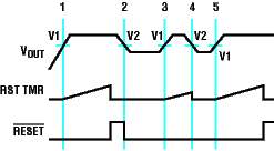
debounce delay. Typical waveforms are shown in Figure 7. On power-up, *RESET
is asserted; it remains low until one debounce delay
(DTD(ms) = 615 • C1(µF)) after FB crosses 1.22V
at time 1. At time 2, FB falls below 1.22V and *RESET is asserted
immediately. When FB exceeds its threshold at time 3, the debounce timer starts,
but FB falls below 1.22V (time 4) before the debounce delay ends and
*RESET remains low. FB crosses 1.22V once more at time 5 and *RESET goes
high one debounce delay later.
To improve noise rejection, the FB
comparator's propagation delay (on a falling edge
at FB) increases from 20µs to 80µs as the differential input voltage
decreases from 175mV to 3mV.
|
Figure 7. Undervoltage monitor waveforms |
Reference and Uncommitted ComparatorThe LTC1642's internal voltage reference is buffered and brought out
to the REF pin. The buffer amplifier should be compensated with
a capacitor connected between REF and ground. If no DC current is
drawn from REF, 0.1µF ensures an adequate phase margin, but larger
capacitors can be used for better suppression of high frequency noise on REF.
The LTC1642 also includes an uncommitted comparator with
an open drain output and a common mode input range that includes ground.
The LTC1642 is a rugged Hot Swap controller that can handle
positive supplies up to 15V. It also provides fast, effective current limiting even
in the presence of a noisy backplane supply, and can protect plug-in
cards against overvoltages up to 33V. |