by Karl Edwards
The size of communication devices is shrinking while data rates continue to rise. Building a small, efficient switching power supply in proximity to sensitive signal circuitry is increasingly difficult. The LT1767 has been designed to address this problem. At 1.25MHz, the switching frequency is above the bandwidth of many systems. If needed, the Sync pin can be used to further increase the operating frequency to 2MHz, keeping switching noise out of any particularly sensitive frequency bands. The high switching frequency reduces the size of the input and output filtering components and allows the use of chip inductors, reducing overall system cost. The lower storage requirements of these filters make possible an all-ceramic-capacitor design.
Inside its MS8 package, the LT1767 provides regulation and control
circuitry along with a high efficiency 0.22W switch. This
small-footprint monolithic approach both reduces board space and simplifies
associated circuitry. Its wide 2.7V to 25V operating supply range and
1.5A maximum switching current limit makes this part ideal in a wide
range of applications. Other useful features of the LT1767 include an
internal undervoltage lockout and a shutdown mode that reduces quiescent
current to 6µA.

Figure 1. Dual-output SEPIC converter |
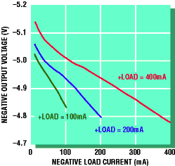
Figure 2. Negative load regulation at several positive loads |
The LT1767 can be used in a variety of high-side switch
converter configurations. The circuit shown in Figure 1 is a dual-output SEPIC
converter, producing both 5V and –5V using only a single magnetic
component. The two inductors shown are wound on a single BH
Electronics toroidal core. The topology for the 5V output is a standard buck
converter. If C4 were not present, the –5V
topology would be a simple flyback winding coupled to the buck converter.
C4 creates a SEPIC topology, which improves regulation and helps
share current between L1A and L1B. Without C4, the voltage swing on
L1B compared to L1A would vary due to relative loading and coupling
losses. C4 provides a low impedance path to maintain an equal voltage swing
in L1B, improving regulation. Figure 2 shows negative load regulation
with constant positive load currents of 100mA, 200mA and 400mA.
Positive load regulation error is insignificant at less than 1%. For more
information on this circuit, refer to Linear Technology Design Note 100. 