|
Ground Planes and Grounding
Designing a high speed ADC system
without using a proper ground is like trying to play basketball on a huge
trampoline. No matter how well you mount the baskets to the court, the
whole court will bounce and wobble as the players jump and try to shoot.
To play the game, you must have a solid floor. Similarly, to give a solid
ground for your data converter circuit, you must use an analog ground plane.
This will put your circuit on a solid foundation.

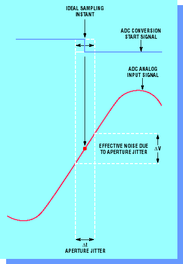
Figure 2. A high performance
ADC layout must have separate analog and digital ground planes, bypass
caps with short connections, and digital outputs routed away from the inputs
Figure 2 shows grounding techniques
for the LTC1410, a 1.25Msps, 12-bit ADC. This provides an example that
can be modified for the particular high performance converter used. All
bypass caps, reference caps and ground connections for the ADC should be
tied to the analog ground plane. Tie them as close together as possible
to reduce the sensitivity to currents that may flow in the ground plane.
The input signal circuitry, filter caps and op amp bypass caps (not shown)
should also be grounded to the ground plane near the ADC.
Noise from digital components
in the system must be kept out of the analog ground. To do this, boards
should be designed with separate analog and digital ground planes, as shown
in Figure 2. (The figure shows a 2-layer board layout. If more layers are
available, separate layers may be used for analog and digital ground planes.)
All noisy digital logic devices must be on the digital ground plane. All
the grounds and bypass caps of the ADC (even the digital ones) should tie
to the analog ground plane. Tie the two ground planes together at only
one point to keep digital currents from taking shortcuts through the analog
ground. The ideal connection point is the ground pin for the ADC output
drivers (or the digital ground pin). If that is not possible, a different
connection point can be used (for example, at the power supply). In any
case, be sure to use only a single connection point.
Supply
Bypassing
The high conversion rates of
high performance converters require proper bypassing on the supply pins.
The key to good bypassing is low lead inductance between the ADC and the
bypass capacitors. The goal is to force AC currents to flow in the shortest
possible loop from the supply pin through the bypass cap and back through
ground to the ground pin.
In Figure 2, the first components
placed around the ADC are the bypass caps, which are located as close as
possible to the supply pins. The capacitors must have low inductance and
low equivalent series resistance (ESR). Tantalum 10µF surface mount
devices are good if they are used in conjunction with 0.1µF ceramics.
Even better are the new surface mount ceramic capacitors, which can be
used alone. They come in values of 10µF or more and have ESR values
as low as 20mW.
Figure 3a shows the differential
nonlinearity (DNL) of the LTC1410 with good supply bypassing. Figure 3b
shows the effects of 2 inches of lead length (corresponding to roughly
60nH of inductance) in series with the supply bypass caps. This is an exaggerated
case of poor bypassing layout, which causes the DNL to degrade beyond 1LSB,
reducing the accuracy to 11 bits. For best performance, use supply bypass
leads of less than one-half inch. A little care pays off with excellent
performance.
Poor layout will degrade the
differential nonlinearity (DNL) of fast ADCs:
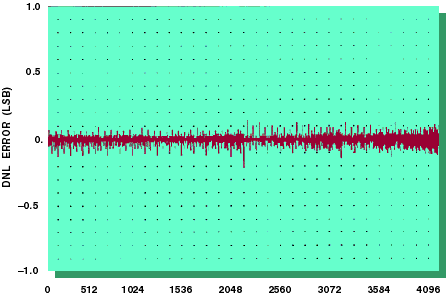
Figure 3a. A Clean LTC1410 layout
with with bypass cap wires of less than 0.5 inch.
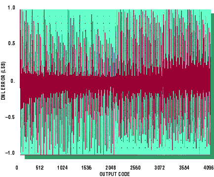
Figure 3b. 2-inch wires to supply-bypass
caps
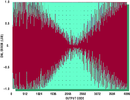
Figure 3c. A wire of more than
2 inches to the reference-bypass cap
Reference
Bypassing
The analog reference input provides
the scale factor for the conversion. For a clean data output the reference
must be stable. Dynamic currents pulled from the reference by the ADC as
it converts perturb the reference unless it is properly bypassed. Surface
mount tantalum or ceramic capacitors provide good results. They should
be located near the reference pin and should be grounded very near the
ADC analog ground pin, as shown in Figure 2.
Figure 3c shows the easily
recognizable signature of a reference bypassing problema bow-tie shape
to the error curve. This occurs because reference perturbations feed in
with full strength for inputs near plus or minus full scale but have less
effect for inputs near zero scale. This degradation in DNL results from
several inches of lead length in series with the reference bypass cap.
Once again, this is an exaggerated case to make the consequences of poor
bypassing more visible. To maintain high accuracy, keep the lead lengths
less than half an inch.
Driving
the Analog Input
Switched
Capacitor Inputs
The inputs to switched capacitor
ADCs are easy to drive if you allow for the fact that they draw a small
input-current transient at the end of each conversion. This happens when
the internal sampling capacitors switch back onto the input to acquire
the next sample. For accurate results, the circuitry driving the analog
input must settle from this transient before the next conversion is started.
There are two ways to accomplish
this. One is to drive the ADC with an op amp that settles from a load transient
in less than the acquisition time of the ADC. Fortunately, most op amps
settle much more quickly from a load transient than from an input step,
so meeting this requirement is not too difficult. The LT1363,
for example, is a good choice for driving the LTC1410 input.
A second solution to handling
the input transient is to use an input RC filter with a capacitor much
larger than the ADC input capacitance. This larger capacitor provides the
charge for the sampling capacitor, which eliminates the voltage transient
altogether. Figure 4 shows such a filter for the LTC1410. The 1000pF capacitor
provides the input charge for the ADC's sampling capacitor. The LT1363's
capacitive load driving capability makes it a good choice for use with
this filter.
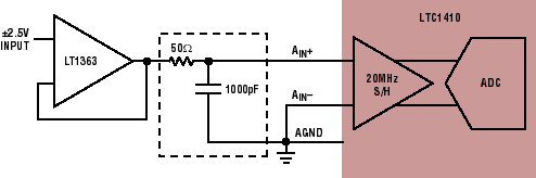
Figure 4. Many new ADCs have
wide-bandwidth sample-and-holds. In lower-bandwidth applications, a simple
RC filter will remove wideband noise that may be present in the input signal
Filter
Wideband Noise from the Input Signal
Many new converters have wide
S/H input bandwidths. This is great for capturing high frequency input
signals, but for lower input bandwidth applications the converter will
pick up any wideband noise that may be in the input signal. To avoid this,
use a filter at the ADC input to pass only your desired signal bandwidth.
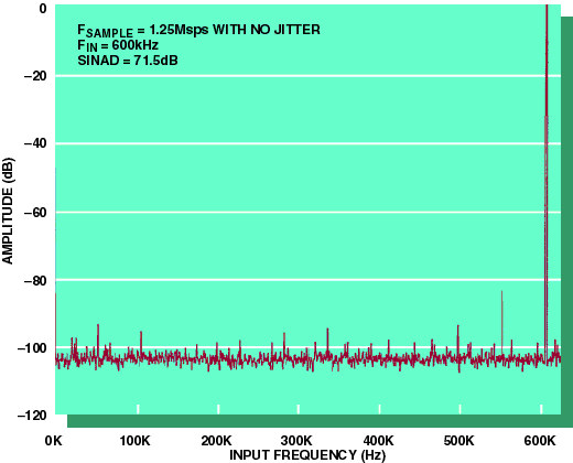
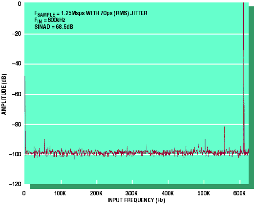
The simple filter in Figure
4 bandlimits the input signal to 3MHz and still allows clean sampling up
to the Nyquist frequency (625kHz). Figure 7a shows the Nyquist performance
of the LTC1410 using this filter. The signal to noise and distortion ratio
(SINAD) is 71.5dB and total harmonic distortion (THD) is �84dB.
Choosing
an Op Amp
To drive high performance ADCs,
you will need a high performance op amp. The noise and distortion of good
ADCs are now so low that they no longer mask the performance of the op
amp. This adds another tradeoff to op amp selection.
High speed, current feedback
op amps have lower DC precision and don't settle as well to high accuracy
(for example, 0.01%) as the voltage feedback types. However, they have
the best distortion and drive for high speed AC frequency domain applications.
Figure 5a shows the FFT result of an LT1227
current feedback amp driving a 172kHz signal into the LTC1410. The distortion
(THD) of �82dB is about 3dB worse than the �85dB of the ADC alone.
High speed voltage feedback
amplifiers have better precision and settling. They work well in frequency
domain applications but are best suited for high speed, time domain or
multiplexed applications where their DC precision and settling are required.
Figure 5b shows the voltage feedback LT1363's 2dB further degradation in
distortion (to �80dB) under the same conditions.
Slower op amps like the OP-27/OP-37
are excellent in noise and precision but are simply not fast enough for
high frequency applications. They distort as they are pushed beyond their
slewing capabilities (as shown in the FFT plot of Figure 5c).
Op amp selection is important
when an ADC has low distortion levels:

Figure 5a. Current feedback
op amps such as the LT1227 (seen here driving the LTC1410) provide the
lowest THD in the FFT output.
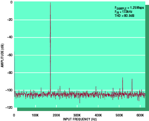
Figure 5b. Fast voltage feedback
op amps do nearly as well in THD as current feedback amps and offer better
precision.
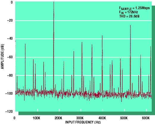
Figure 5c. Slower op amps pushed
beyond their slew limits will severely distort fast signals.
Driving
the Convert-Start Input
An improperly driven conversion-start
input can create conversion errors in a couple of ways. First, if an ADC
has internal timing, the returning edge of the convert signal (the opposite
edge from the one that starts the conversion) can couple noise into the
converter if it occurs during the conversion time. To avoid this, use a
narrow pulse for convert-start instead of a square wave. This ensures that
it either returns quickly (after the sample is taken but before the conversion
gets underway), or returns after the conversion is over. (This does not
apply to those ADCs that draw all their timing from a clock input and require
precise 50% duty-cycle clock inputs.)
A convert-start signal that
overshoots or rings can also degrade performance. If it overshoots beyond
the supply rails it can turn on the ADC's input protection diodes and couple
noise into the converter. If it rings, it may still be bouncing around
as the ADC's sample-and-hold captures the input signal, which can affect
the conversion result. Normally, overshoot and ringing are not a problem
with high speed CMOS logic on a well designed board but they are still
things to watch out for. |
|