by John Seago and Ajmal Godil
Introduction
Active voltage positioning is a technique that can be used to save
cost and space by reducing the number of output capacitors required to meet
a microprocessor's power supply requirements. Total system cost
and required PCB space are important aspects of today's portable
equipment designs, so decreasing the number of large, expensive output capacitors
is worth some effort. Both the LTC1735/LTC1736 current mode
switching regulator controllers (Linear Technology
IX:1, February 1999, pp. 1, 3–5, 35) and the
LTC1702/LTC1703 voltage mode controllers (Linear Technology IX:3, September 1999, pp. 16–20) can take advantage of active voltage positioning.
Microprocessors frequently change their load current requirement
from almost no load to maximum load current and back again very quickly.
The rising and trailing edges of these load current steps exceed the
bandwidth of the switching regulator control loop. Currently, a typical load step is
either 0.2A to 12A in 100ns or 12A to 0.2A in 100ns. The core voltage of
the microprocessor must be held to about ±0.1V of nominal in spite of these
load steps.
Since the switching regulator control loop cannot respond in
100ns, the output capacitors must temporarily supply the load current
when the output current increases rapidly. Also, the output capacitors must
absorb the energy stored in the inductor when the output current
decreases rapidly. Capacitor ESR and ESL primarily determine the amount of
droop and overshoot in the output voltage caused by a load current step.
Normally, several capacitors in parallel are required to meet the
microprocessor load transient requirements.
Active voltage positioning is a form of deregulation. It sets the output
voltage high for light loads and low for heavy loads. In the
low-current-to-high-current transition, the output voltage starts at a voltage higher
than nominal so the output voltage can sag more and still meet the
minimum output voltage specification. By setting the output voltage lower
than nominal for heavy load conditions, more output voltage variation is
possible when the load current suddenly decreases to almost zero. Less
output capacitance is required because more output voltage variation is allowed
on the output capacitors.
The implementation of active voltage positioning depends on the
type of OPTI-LOOPTM error amplifier used in the switching regulator. With
the LTC1736, connecting two resistors to the
ITH pin adjusts the output voltage to decrease as load current increases. This technique will only work with a current mode
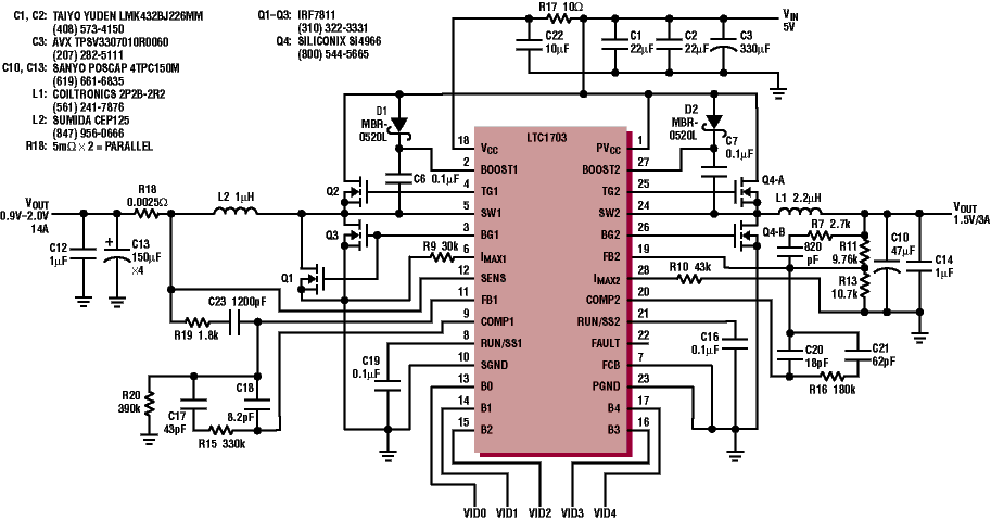
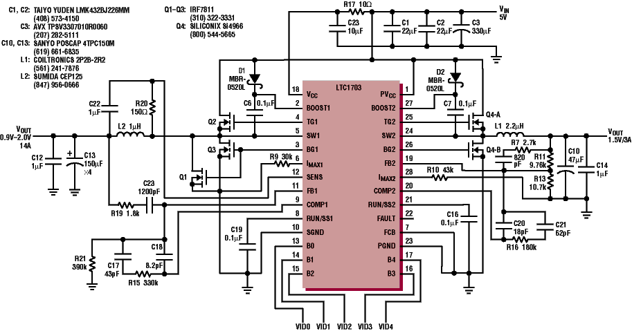
control regulator. Different techniques are available for the LTC1703;
these can also be used on the LTC1736 and will be discussed later.
Reducing output capacitance with active voltage positioning
requires connecting two resistors to the
ITH pin and readjusting the loop
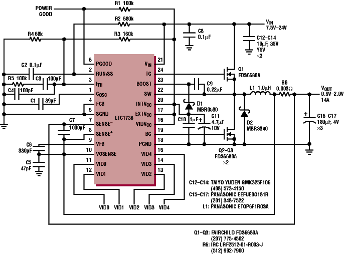
compensation component values. Figure 1 shows a core voltage regulator
circuit designed to operate from a 7.5V to 24V input and provide ±7.5%
accuracy to VID controlled output voltages from 0.9V to 2.0V with load
current steps from 0.2A to 12A. Although 7.5% output voltage accuracy
does not sound very impressive, 7.5% of 1.4V is only 105mV, and includes
setpoint accuracy and load and line regulation, as well as margin for
transient response to the 12A load step.
The circuit in Figure 1 is a current mode, synchronous buck
regulator with a switching frequency of 300kHz. The nominal output voltage is
selected by the standard INTEL mobile VID code. The actual output voltage
varies as a function of the load current. The no-load output voltage from
this circuit is higher than nominal because the current sourced by
R3 creates a positive offset bias at the input of the transconductance
error amplifier. The error amplifier current sourced into R4 develops a
negative input offset bias voltage. This negative offset causes the output
voltage to be less than nominal under full load conditions.
Forced offsets at the input of the error amplifier should be limited
to ±30mV. If a lower output voltage is required at full load, the voltage
drop across the current sense resistor can be subtracted from the regulated
output voltage by connecting the
VOSENSE pin to the inductor side of the
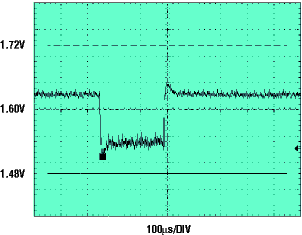
sense resistor, as shown in Figure 1. Figure 2 shows a transient waveform resulting from a 12A load step.
The output voltage tolerance of 7.5% allows a ±120mV variation.
Microprocessor Load Steps
How Active Voltage Positioning Works
LTC1736 Circuit with Active Voltage Positioning