ADSL Line Driver/Receiver Design Guide,
|
by Tim ReganIntroductionConsumer desire for faster Internet access is driving the demand for
very high data rate modems. A digital subscriber line (DSL)
implementation speeds data to and from remote servers with data rates of 512Kb/s
to 8Mb/s, much faster than current 56Kb/s modem alternatives.
This speed of data communication is providing the Internet with the
capability to transfer information in new formats such as full-motion video,
while greatly improving the timeliness of conventional information access.
One very important feature of DSL technology is that the connection
is handled through a normal telephone line; therefore, no special high
speed cables or fiber optic links are required and every home and office is
most likely DSL ready. Another feature is that the data interface can
operate simultaneously with normal voice communication over the same
telephone line. This allows the modem to be connected at all times and
not interfere with the use of the same line for normal incoming and
outgoing phone calls or faxes.
The real "magic" of DSL technology stems from the application of
digital signal processing (DSP) algorithms and data coding schemes. The
implementations have built-in intelligence to accommodate the wide
variations of data transmission signal conditions encountered with each
connection through the telephone switching network. Sophisticated ASICs have
been developed to provide small modems for PCs and handheld devices and
the ability to compact many DSL lines on a single PCB card for telephone
central-office deployment.
However, as is the case with almost any system, DSL still requires
fundamental operational amplifier functions to put the signal on to the phone
line and to pick off the small signals received at the other end.
Although many system designers are competent and comfortable with DSP
and all things digital, they often find their understanding of analog issues to
be a bit rusty when it comes to implementing the physical connection
to and from the telephone line. This series of articles will provide an
overview of the requirements placed on the amplifiers and provide
guidelines to component selection and the implications on distortion performance
and power consumption and dissipation, the most important system
issues related to the analog components.
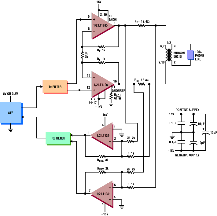
Figure 1 shows a complete central office DSL line driver/receiver. This
is the basic circuit topology that provides differential transmit signal
drive to the line and detection of the differential received signal. The
full requirements of DSL are easily met by using devices from Linear
Technology's broad line of high speed power amplifiers for the driver and
high speed, low noise dual amplifiers for the receiver. Using either current
feedback or voltage feedback topologies, the family of drivers consists
of amplifiers with bandwidths from 35MHz to 75MHz, slew rates in
excess of 200V/µs with output current capability from 125mA to over 1
Amp. The receiver family combines similar high speed performance with
low noise, less than 10nV/(Hz1/2), and low quiescent operating current, less
than 10mA. The devices shown in Figure 1 are the LT1795 500mA output
current, 50MHz bandwidth dual op amp and the LT1361 50MHz dual
amplifier with input noise voltage of 9nV/(Hz1/2) and total supply current
of only 10mA.
Although there are several variations of DSL technology (SDSL,
HDSL, HDSL2, VDSL and ADSL, to name a few) the requirements placed on
the amplifiers for these different standards are very similar. The
major difference between the approaches, as they affect the line driver, is
the amount of power actually put on to the phone line by the
line-driver amplifier. For simplicity, these
articles will focus on the most recently approved standard, ADSL
(asymmetric DSL), but the concepts discussed apply equally to any of the
other standards.
This first installment will provide an overview of the requirements
of ADSL and how it is done, as well as a discussion of the circuit topology
and the requirements for the components used for implementation.
The full specifications for ADSL are contained in two ITU
(International Telecommunications Union) documents called G.992.1, for
systems often referred to as Full-Rate ADSL or G.dmt, and G.992.2, a lower data
rate approach often called G.Lite. Both systems use a technique
called discrete multitone, or DMT, for transmitting data. With DMT, a
frequency band up to 1.2MHz is split up into 256 separate tones (also call
subcarriers) each spaced 4.3125kHz apart. With each tone carrying
separate data, the technique operates as if 256 separate modems were
running in parallel. To further increase the data transmission rate, each
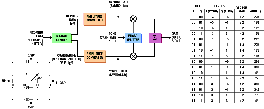
individual tone is quadrature amplitude modulated (QAM). As shown in
Figure 2, the data to be transmitted is used to create a unique
amplitude and phase-shift characteristic for each carrier tone, through the
combination of I and Q data, called a symbol. The symbols represented by each
tone are updated at a 4kHz rate or 4000 symbols per second. Full Rate
ADSL uses up to 15 bits of data to create each symbol. This results in a
theoretical maximum of 60Kb/s for each tone. If all 256 tones are used
in parallel, the total theoretical data rate can be as fast as 15.36Mb/s.
For G.Lite, only 8 bits are used per symbol with only half of the carrier
tones used for a theoretical maximum data rate of 4.096Mb/s.
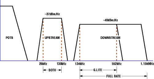
In an actual DSL application, the tones are allocated for use
depending on the direction of communication, as shown in Figure 3. Most of
the tones are used for communication from the central office (CO) to an
end user's PC modem (often referred to as the CPE or customer
premises equipment). This direction of communication is called
"downstream." The direction of communication
from a PC modem to the central office (and, ultimately, to an Internet server)
is called "upstream." The use of more tones for the downstream
direction makes sense from an Internet-access point of view, because most
users download more information than they upload. Most upstream
communication with a server is simply to request information to be sent quickly
downstream. This difference in data rates up- and downstream is the
reason ADSL is called asymmetric DSL.
|
Figure 3. DMT channel allocation |
Also indicated in Figure 3 is the power spectral density (PSD) of all of the tones used. This determines the amount of signal power that needs to be put on to the phone line. The power levels are restricted to minimize crosstalk and interference into other phone lines contained in wire bundles en route to and from the central office. The total power required can be determined from the following equation: |
|
LINE POWER (dBm) = PSD (dBm/(Hz1/2)) + 10 ·
Log(FMAX FMIN)
The downstream power requirements are much higher than
the upstream requirements because of the wider bandwidth used for
the transmission. For this reason, Full Rate ADSL requires more line
power than G.Lite for downstream transmissions. Upstream power is the
same for both Full Rate and G.Lite implementations. As will be seen,
the line power requirement is the most significant factor in designing a
line driver for a particular application.
Table 1 is a summary of the characteristics, electrical
requirements and maximum data rates for ADSL modems.
The following are important items to note:
The phone line characteristic impedance for ADSL is 100. This
is used to determine the voltage and current required to provide the
proper line-power level.
The term PAR stands for peak-to-average ratio. This term is similar
to the more common term of crest factor. This determines the peak value
of the voltage put on the line over time with respect to the RMS voltage level:
VPEAK = PAR · VRMS
The DMT signal placed on the line looks basically like white
noise, because many different frequencies of rapidly changing amplitude
and phase are combined simultaneously. The changes of each tone are
considered random as they result from an arbitrary sequence of data bits
comprising the transmitted information. Over time, the signals can align
and stack up to create a large peak signal. If this large peak is not
processed cleanly (for example, if the line-driver amplifier clips) data errors can
occur, which must be detected and resent. Transmission errors, particularly
over a noisy environment such as phone lines, are inevitable. These errors
are identified by a term called the bit-error rate (BER); an acceptable
level to maintain fast and accurate data transmission is one error per
every 107 symbols. The PAR is
determined by the probability of the random line signal reaching a certain peak
voltage during the time interval required for
107 symbols. For the DMT signal, this peak value is 5.3 times the RMS
signal level. This factor is very important in determining both the
minimum supply voltage required to prevent clipping of the signal and also
the peak output current capability of the line driver.
Although the data rates shown in Table 1 are impressively fast,
they are, indeed, theoretical. In an actual connection over the phone line,
all manner of interference sources will alter the frequency response over
the 1.2MHz band. These interference sources can contaminate or
attenuate many of the carrier tones to render them completely unusable, or
useful but with less than the maximum possible number of data bits
encoded. Additionally, higher frequency tones are attenuated more than the
lower ones, particularly over longer lengths of phone line used to make
the connection.
Another issue that can render particular tones unusable or
create transmission errors is distortion from the amplifier driving the line.
Distortion products, whether harmonic, intermodulation or from signal
clipping, from any of the carrier tones, create signal energy in the
frequency spaces used by other tones. This energy also contaminates the
data content of the tones and can result in fewer tones being used for data
transmission. If many tones are unusable or their data handling capability
is reduced, the actual data rate for any given connection can be
significantly less than the theoretical maximum.
| |||||||||||||||||||||||||||||||||||||||||||||||||||||||||||||||||||||||||||||||
|
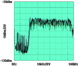
One of the best features of a DSL modem is the intelligence built in to obtain the fastest data rate for any set of line conditions. When a connection between a modem and the telephone central office is initiated, the first action to occur is called "training-up." During this interval, both ends transmit maximum power in each channel in an effort to determine which channels are best suited for use. The DSP algorithms will automatically pack the most data into the best transmission channels to maximize the data rate for a particular connection. Figure 4 illustrates a typical line spectrum during a training-up interval in a G.Lite example, as measured at the central office end. |
Figure 4. G.Lite training-up spectrum |
A Typical ADSL Line Driver/Receiver CircuitReferring to Figure 1, the components shown will implement a
Full Rate ADSL central office (downstream) port. A discussion of the circuit
topology and aspects important for component selection follow.
A transformer is used to connect the transceiver to the phone line,
mainly to provide isolation from the line. The turns ratio of the transformer can
be used to provide gain to the transmitted signal. This turns ratio has
a major effect on the power supply voltages for the line-driver amplifiers.
By stepping up the signal from the driver to the line via the transformer,
the amount of voltage swing needed by the amplifiers is reduced. As an
ideal transformer has equal power in the primary and secondary, while
the voltage is stepped up, the current is stepped down. The consequences
of using a step-up transformer are beneficial in that lower, more
conventional supply voltages can be used, but the amplifiers must have higher
current driving capability.
The limit on the turns ratio is primarily a function of the
sensitivity of the receive circuitry. Step-up transformers will, unfortunately,
step-down the signal received from the phone line. Further attenuation
of the received signal by the transformer in addition to the inherent
transmission line attenuation can cause the receiver to stop functioning. If
this occurs the modem will disconnect from the line.
A transformer should be selected for a flat, distortion-free
frequency response from 20kHz to 2MHz to cover the full frequency spectrum for
an ADSL transmission. Minimal insertion loss in the transformer over
the same frequency range is also desirable. Insertion loss, usually
specified in dBm, is power lost in the transformer. The driver amplifier
must provide this additional power in order to maintain the required signal
power level on the phone line.
The two resistors (called back-termination resistors) shown between
the amplifier outputs and the primary of the transformer are inserted for
two reasons: to provide a means for detecting the received signal and
to make the impedance of the modem match the impedance of the
phone line. The receiver circuit is two difference amplifiers that provide gain
to the small signals that appear across the termination resistors. The
connection and scaling of the input resistors to the receiver amplifiers
are purposely set to provide a first-order cancellation of the
simultaneously occurring transmit signal. This technique is called "echo
cancellation" and the circuit topology is called a
"2-wire to 4-wire hybrid" (the 2-wire phone line interfaces with four
wires, the two differential driver lines and the two receive signal lines). The
cancellation of the transmitted signal from the received signal path is not
perfect. Due to signal phase shifts and resistor mismatching, a factor of 6dB
to 20dB of attenuation is typical, with higher frequencies being
cancelled less. The amount of transmitted signal that remains is cancelled
digitally by DSP echo-canceling algorithms.
The value of the termination resistors is a function of the line
impedance and the transformer turns ratio. The turns ratio,
n, is defined by the number of turns of the winding
connected to the phone line (the secondary) divided
by the number of turns of the driver side winding (the primary).
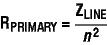
To make the modem impedance match the line impedance, the total
impedance across the primary winding is determined by the
following relationship: To provide balanced drive to the primary of the transformer, so
that each power amplifier shares the work load evenly, each termination
resistor is set to a value of one-half of
RPRIMARY.
This value of termination resistance on the primary is also
optimal for receiving maximum power from the line. The received signal on
the phone line, eRX, driving the
secondary through the line impedance,
ZLINE (nominally 100) will develop
signal power in the primary per the following relationship: which is also at a maximum when While the termination resistors serve an important purpose, they
also create significant signal and power loss. With the resistors set to
their proper value, one-half of the power delivered by the amplifiers is
dissipated in these resistors. To deliver 100mW of signal power to the
phone line, for example, requires the driver amplifiers to output at least
200mW of power.
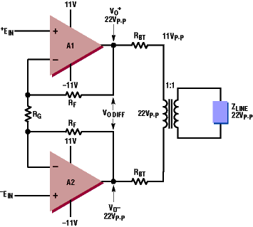
Two amplifiers configured as a differential gain stage are typically used
to provide signal drive to the primary of the transformer. There are two
reasons for this configuration; it reduces the supply voltage to the amplifiers
by a factor of two and also cancels any even harmonic distortion
nonlinearity contributed by the amplifiers.
With single-ended drive of the primary, the supply voltage for
the amplifier must be large enough to provide the full peak-to-peak
signal swing of the DMT signal placed on to the phone line. With differential
drive, each amplifier contributes just one-half of the peak signal
amplitude; therefore, the total supply voltage is only one half the peak-to-peak
voltage level placed on the line. This is shown conceptually in Figure 5.
This reduction in supply voltage allows the use of the standard power
supply voltages available in computers for the high speed DSL modem card.
|
Figure 5a. A single-ended driver requires a high supply voltage to produce the desired peak-to-peak swing of the DMT signals on the phone line. |
Figure 5b. A differential drive achieves the same swing with half the supply voltage of the single-ended driver.
|
|
A differential amplifier will ideally cancel all even harmonic
distortion products. This is due to the application of a signal that is the
difference between two signals, one signal being an inverted version of the other, to
the primary of the transformer. This can be shown mathematically by
representing the linear output signals of the amplifiers as a power series:
Each output is a linear function of the input signal:
VO = f(EIN)
which, represented as a power series, is
VO = a1EIN +
a2EIN2 +
a3EIN3 +
a4EIN4 +
a5EIN5...
The inputs to the differential amplifier are
+EIN and EIN; therefore:
VO(+) = a1EIN +
a2EIN2 +
a3EIN3 +
a4EIN4 +
a5EIN5...
and
VO() =
a1EIN +
a2EIN2
a3EIN3 +
a4EIN4
a5EIN5...
The differential output of the amplifier stage is
VODIFF = VO(+)
VO()
therefore:
VODIFF =
2a1EIN +
2a3EIN3 +
2a5EIN5 + ...
which does not contain any even harmonic products. The
complete cancellation of even harmonics depends on the gain and
phase-shift matching of the amplifiers and the signal paths over the frequency
range of concern.
High speed amplifiers with bandwidths much wider than
the transmitted signal bandwidth should be used to maintain flat gain
and constant phase shift of the DMT signals. The amount of gain required
in the transmit power amplifiers is dependant on the signal levels
provided by the analog front end (AFE), which is a circuit block that
provides the interface between the line transceiver and the DSP processor.
The gain must be sufficient to put the proper amount of power on the
phone line for the DSL standard being implemented (refer to Table 1).
The maximum frequency to be processed by the amplifiers is also a function
of the standard being applied; this, in turn, sets the minimum
bandwidth required. As a rule of thumb, the gain bandwidth product specification
of the amplifiers used should be at least five times the required value
to maintain linear accuracy over the transmitted signal spectrum.
This specification provides an indication of the distortion-free, high speed
signal processing capability of the amplifier. For example, a Full
Rate ADSL downstream transmitter with a gain of four and a maximum
frequency of 1.1MHz requires a gain-bandwidth of 4.4MHz; therefore,
amplifiers should be chosen that have a gain-bandwidth specification of at
least 22MHz. Parts with higher bandwidths are even better for preserving
excellent gain and phase shift matching over the 1.1MHz band of operation.
The slew rate of the amplifiers used is not so critical, because the
signal spectrum is typically band-limited by filter networks. The step response
of these filters slows down the rise and fall times of the signals presented
to the amplifiers. A slew rate of at least 10V/µs is usually adequate.
However, very fast slew rates are essentially free in wideband amplifier
designs. Internal biasing currents charging and discharging internal
compensation capacitors and individual node capacitances of the circuit
determine the slew rate of an amplifier. To produce a high frequency
amplifier, circuit-biasing currents are increased to minimize impedances at
critical circuit nodes and small geometry transistor structures are used to
minimize stray capacitance. This results in very fast slew rates for the amplifier as
an inherent byproduct of a high gain-bandwidth product
characteristic. Faster slew rates ensure very fast dynamic response and reduced
signal distortion.
Low noise characteristics, together with a wide gain bandwidth
capability are most important for the amplifiers used in the receive
circuitry. On a typical connection, a phone line will have a noise
floor power spectral density of 140dBm/(Hz1/2). This is equivalent to a noise
voltage of 31nV/(Hz1/2). The receiver amplifier should have a noise
spectral density in the band between 20kHz and 1MHz lower than this
level. Linear Technology provides several fast amplifiers with noise voltage
spectra of less than 10nV/(Hz1/2). Lower noise is required in inverse proportion
to the turns ratio of the transformer used to address the attendant
reduction in both the noise floor and the received signal.
|
|
The amount of signal received is a function of the length of phone line used to make the connection, as shown in Figure 6. This is referred to as the loop length. Very long loop lengths can severely attenuate the transmitted signal, particularly at the higher channel frequencies. The greater the attenuation of a channel, the fewer data bits can be transmitted in that channel, which affects the overall communication data rate. As a rule of thumb, a received signal-to-noise ratio of 18dB allows two data bits to be used in a channel. With each 3dB of additional signal above the noise floor, an extra bit of data can be used. With 45dB to 50dB signal-to-noise ratio, a full 12 bits of data can be exchanged in one channel frequency. |
Figure 6. Typical received signal power spectral density, AWG 26 loops. |
|
The next installment in this series will provide the design calculations
to determine the minimum requirements for supply voltage, current
drive capability and resultant power consumption and dissipation. In
addition, heat management issues will be discussed. |