by Ajmal Godil
In some applications, it is necessary to select and
hot swap the higher of two supplies and generate a
regulated output voltage from the selected supply. If only one
input supply is present, the circuit should select it and
generate the same output voltage. The term "hot swapping" refers
to plugging a circuit board into or removing it from a
live backplane. When this is done, the supply bypass
capacitors on the board can draw huge transient currents from
the backplane power bus as they charge. The transient
currents can cause permanent damage to the connector
pins and cause glitches on the system supply, causing
other boards in the system to reset. A circuit based on
an appropriate LTC Hot SwapTM controller can eliminate
these problems.
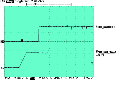
The circuit in Figure 1 selects between and hot swaps
a 3.3V and a 5V input supply and generates a constant
3.3V output supply using the LTC1645 and the LTC1735.
The LTC1645 is a 2-channel Hot Swap controller and
the LTC1735 is a synchronous step-down switching
regulator. The two voltage supplies,
VIN1 and VIN2, are fed into
the LTC1645 Hot Swap circuit, where the higher of the two
supplies is selected (VOUT_HOT_SWAP) and then fed into the
LTC1735 DC/DC converter. The LTC1735 circuit generates a
constant 3.3V output voltage, regardless of whether its input
is 3.3V or 5V. To simplify the circuit description, the
operation of the LTC1645 and the LTC1735 will be discussed
separately.

Figure 1. 3.3V/5V Hot Swap circuit plus LTC1735 SEPIC converter
LTC1645 Hot Swap Operation
Back-to-back MOSFETs Q1 and Q2 are connected to
the VIN1 (5V) supply and Q3 and Q4 are connected to the
VIN2 (3.3V) supply. The reason for using back-to-back
MOSFETs is to keep the internal body diodes from shorting the 5V
and 3.3V supplies together. The LTC1645's Gate1 pin
controls Q3 and Q4 and its Gate2 pin controls Q1 and Q2. The
ON pin has a 0.8V turn-on threshold for Gate1 and a 2.0V
turn-on threshold for Gate2. The VCC1 and
VCC2 pins have 2.3V and 1.2V undervoltage lockout thresholds,
respectively. Since the circuit in Figure 1 selects between two
supplies, the following two cases are possible:
When the 5V and 3.3 supplies are present on
VIN1 and VIN2, respectively,
VCC1, VCC2, Sense2, and
Sense1 are pulled up to approximately 4.7V by D1, which clears the
undervoltage lockout thresholds of VCC1 and
VCC2. The COMP+ pin is pulled up to
2.5V by the voltage divider formed by R2 and R6. Since the voltage on
the COMP+ pin (noninverting terminal of the onboard comparator) is
greater than 1.24V, the COMPOUT pin (open drain output of the comparator)
is pulled up to 5V by R7. This turns on Q5 and pulls the gates of Q3 and
Q4 to ground. The On pin is pulled up to approximately 2.74V through R1,
R4 and R8. After one timing cycle (t = C2 · 1.24/2µA), an internal 10µA
current source from the charge pump is connected to the Gate1 and
Gate2 pins. The Gate1 pin is pulled to ground by Q5 and the voltage on
the Gate2 pin starts to rise, with a slope given by dV/dt = 10µA/C1. The
internal charge pump guarantees that the Gate2 voltage will rise to
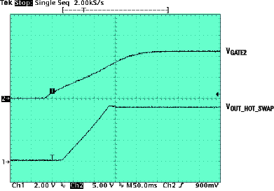
approximately 12V. As the Gate2 voltage rises to about 1V, Q1 and Q2
start conducting and VOUT_HOT_SWAP
starts rising. The output voltage will eventually rise to the input supply,
which is 5V. Figure 2 shows the Gate2 pin and
VOUT_HOT_SWAP voltages rising to 12V and 5V, respectively.
Case One: 5V and 3V Supplies Present