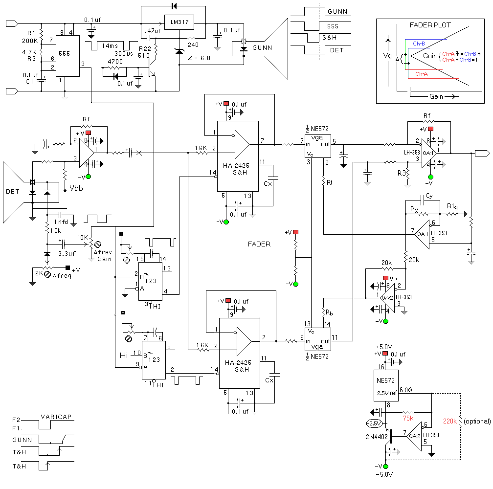
Several components don't have values in Glen A. Williamson's schematic. A good starting point would be:
Cx = 1000 pF low-leakage film Cy = 0.47-2.2 µF Ry = 100 kΩ R1g = 10 kΩ Rt = 10-22 kΩ Rb = 10-22 kΩ 74123 R&C = S&H Timing = 1000 pF and 10 kΩ NE572 Input Res = 20 kΩ NE572 Output Cap = 100-470 pF low-leakage film LF353 Diff. Amp = All 10 kΩ (use external amp for audio gain/headphones) OA-1 Unmark Cap = 10 µF OA-1 Unmark Res = 47 kΩ Gain Control (Fader) = 10 kΩ |
(AI Assisted)
Based on a circuit analysis of this microwave transceiver / dual-channel Doppler radar (which pulses a Gunn diode source, samples two receiver phases/frequencies via dual HA-2425 sample-and-holds, and balances/fades the channels using an NE572 compandor/VCA, here is a functional breakdown with recommended component values for the missing labels.
Dual Monostable Pulse Generators (74123)
Function: Generates short sampling trigger pulses (logic LOW on HA-2425 pin-14 triggers the sample/track mode synchronized to the 555-driven Gunn diode pulse.
The Gunn pulse is 300 µs so the S&H sampling pulse width must be significantly shorter than 300 µs (typically 1 to 10 µs)
For standard 74HC123/74LS123, pulse duration is given by: t ≈ 0.45 * Rext * Cext
Set Cext to 1000 pF.
Set Rext with a 10k trimpot.
Trim to approximately 0.5 to 5 µs pulses.
Sample-and-Hold Stages (HA-2425)
Function: Holds the signal during the active transmit/receive microwave return pulse.
Per the HA-2425 datasheet, hold capacitor Cx controls droop rate vs. acquisition time.
A value of 1000 pF provides an acquisition time of provides an acquisition time of approx. 4 µs with low droop rate (polystyrene, polypropylene, or NP0/C0G ceramic or low dielectric absorption).
Compandor / Fader Stage (NE572)
The NE572 variable gain cell input impedance is typically driven via an external resistor that scales the input current: Iin = Vin / Rin
Typical value 20 kΩ for approx 1V peak input signals.
Two variable gain amplifiers (VGAs) acting as complementary gain controls: CHA + CHB = 1
Reference divider at Vc to +V and -V. Sets the control voltage midpoint. With symmetric supplies, two matched resistors 10 kΩ to +V and 10 kΩ to -V.
NE572 gain control resistors Rt and Rb driven from the fader loop op-amp. Typical NE572 tracking/bias resistors into pins 2 and 14: 10-22 kΩ
NE572 output filter capacitors (pins 5 and 11 to ground): 100-470 pF
Bottom Loop / Integrator Amp
R1g = input/reference to ground 10 kΩ
Ry = 100 kΩ (feedback resistor)
Cy = (integrator/averaging cap) 0.47-2.2 µF (sets the slow thermal/AGC fading time constant so the circuit smoothly crossfades between channels without modulating audio/Doppler frequencies).
AC feedback divider (from main output back to integrator): resistor 47 kΩ, capacitor to ground: 10 µF