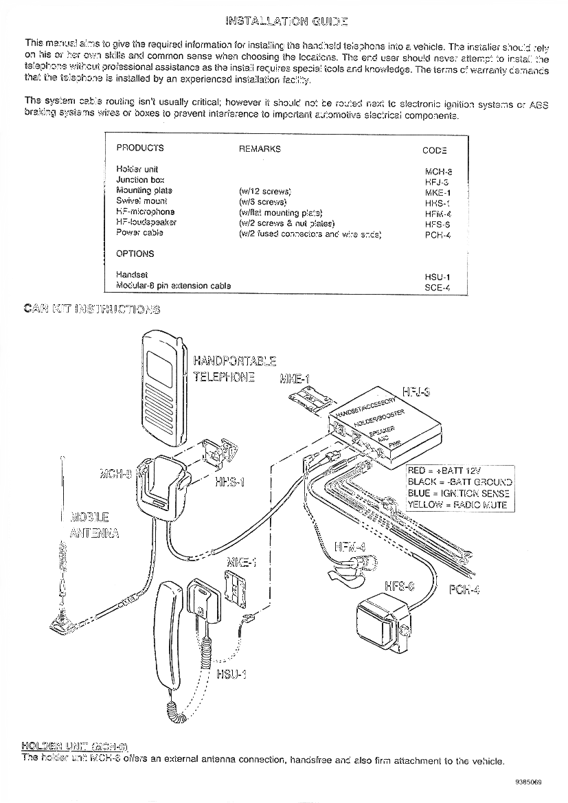
Please forgive the poor diagram. This diagram has be drawn as if you are
looking at the bottom of the phone with the keypad to the top.

( o ) = Charging Connector
( )   = A spacing hole
|     = Battery Terminal
(O)   = Antenna Connection
I     = Pin Block. The Pins are numbered as shown

              1             8
  ( o ) ( ) | I-I-I-I-I-I-I-I (O) |
              9             16

  The connector uses the X100 protocol. This a complex protocol. It's is
  NOT just a matter of connecting some pins and that's it. If you have
  a copy of the X100 protocol please e-mail it to me so all to enjoy.

  Description of X100

  PIN     Name                    Description
  ---     ----                    -----------
  1,9     GND                     Digital ground
  2       MIC/JCONN               External audio input from accessories or
                                  handsfree microphone. Multiplexed with
                                  junction box connection control signal
  3       AGND                    Analogue ground for accessories
  4       TDA                     Transmitted DBUS data to the accessories
  5       M2BUS                   Serial Bidirectional data and control
                                  between the handportable and accessories
  6       HOOK/RXD2               Hook indication. HP has a 100KE pull-up
                                  resistor.
  7       PHFS/TXD2               Handsfree device power on/off, data to
                                  flash programming device.
  8,16    VCHAR                   Battery charging voltage
  10      EAR/HFPWR               External Audio output to accessories or
                                  handsfree speaker
  11      DSYNC                   DBUS data bit sync clock
  12      RDA                     DBUS recieved data from the accessories
  13      BENA                    Power supply to headset adapter
  14      VF                      Programming voltage for FLASH
  15      DCLK                    DBUS data clock

As you can imagine. YOU CAN DESTROY YOUR NOKIA BY FOOLING AROUND WITH THESE
CONNECTIONS. Therefor I accept NO responsability for any possible damages. My
advice to you is to think twice before doing something and if you are going to
try make use of a car-kit holder to get access to the X100 connector since it
is to tiny to use a self-fashioned connector.

IT IS POSSIBLE TO REPROGRAM THE NOKIA 2110 as is indicated by the pinout
description so watch it !

  Sourced from Hans Engelen . Thanks Hans!
I'll leave it up the reader to make it. But the important charging current needed is below
NOTE!! I take no responsibility for this information!!The Nokia mains powered charger delivers 12Vdc current limited to 770mA or to 0.77A - yes zero point seven seven. End of charge detection is done by the phone itself. Note that connecting 12Vdc without current limiting to the phone is likely to damage either or both the phone and the battery. Sometimes the phone will display "not charging", other times the switching transistor inside the phone will die. NOTE: As of the Nokia 1610 the charger has CHANGED! The charger now supplies 10Vdc at 740mA
I'm sorry for the size of these but if I re-size them you won't be able to
read the text.
Simple.
Pay the money and purcahse them from your local standards office. It is COPYRIGHTED material, therefor it is NOT available on the internet. Before you ask, no I don't have a copy of it.
Table of contents of this chapter, General table of contents
Top of the document, Beginning of this Chapter